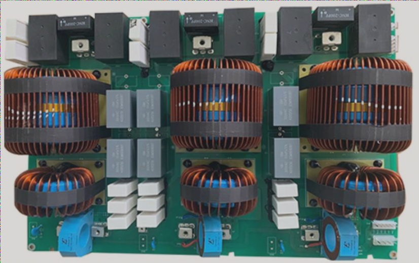
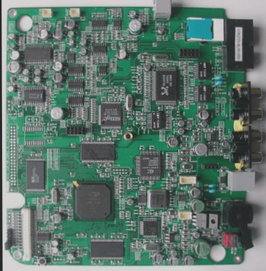
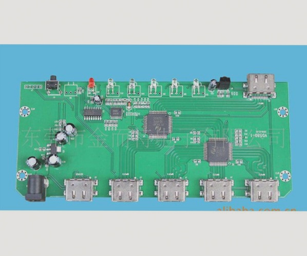
1. PCB design should follow a structured order, such as proceeding from left to right and from top to bottom.

2. The width of the PCB traces and the trace spacing should be optimal, and the gap between the capacitor pads should be as consistent as possible with the distance between the capacitor leads.

3. When creating the PCB layout, minimize the number of bends in the traces, keeping the routing as simple and clear as possible.

4. Pay close attention to the sequence of pin placements when designing the PCB layout, ensuring that the spacing between component pins is reasonable.

5. **PCB Wiring Direction:**

From the perspective of the soldering surface, component placement should align closely with the schematic diagram, and the wiring direction should follow the layout shown in the circuit diagram. This alignment facilitates easier inspection, debugging, and maintenance during the production process, as various parameters are typically tested on the soldering surface. (Note: This refers to the requirement that circuit performance, installation, and panel layout of the entire system are met.)

6. **Design Considerations:**

While ensuring the circuit’s performance requirements, the design should prioritize efficient wiring, minimize the use of external jumpers, and route the wires smoothly according to best practices. The layout should aim to be intuitive, easy to install, and straightforward for maintenance and repair.

7. **Component Arrangement:**

The distribution of components on the PCB should be reasonable and evenly spaced, aiming for a neat, aesthetically pleasing, and structurally sound layout.

8. **Orientation of Input and Output Terminals:**

(1) The distance between associated lead terminals should be minimized, typically around 2-3/10 inches for optimal routing.

(2) Input and output terminals should be clustered on one or two sides of the PCB, avoiding excessive dispersion.

9. **Placement Guidelines for Potentiometers and IC Holders:**

(1) **Potentiometers:** Potentiometers are used to adjust output voltage in voltage regulators. When designing, ensure the potentiometer is set to increase output voltage when fully rotated clockwise, and decrease output voltage when turned counterclockwise. In adjustable constant current chargers, the middle potentiometer adjusts the charging current. As the potentiometer is rotated clockwise, the current should increase. The potentiometer should be positioned to fit the overall system structure and panel layout, ideally on the board’s edge with the rotating knob facing outward.

(2) **IC Holders:** When designing the PCB, special care should be taken when placing IC holders. Ensure the positioning slot on the IC holder is oriented correctly, and verify that each IC pin is positioned properly. For instance, the first pin must always be located at the lower right or upper left corner of the IC socket, adjacent to the positioning slot (viewed from the soldering surface).

10. **Resistor and Diode Placement in PCB Layout:**

PCB design typically includes two placement orientations: horizontal and vertical.

(1) **Horizontal Placement:** When the circuit has fewer components and the PCB is relatively large, horizontal placement is preferred. For resistors below 1/4W, the standard pad distance is about 4/10 inches; for 1/2W resistors placed horizontally, the distance between pads is typically 5/10 inches. For diodes placed horizontally, such as 1N400X series rectifiers, the pad distance is usually 3/10 inches, while for 1N540X series rectifiers, it is generally 4-5/10 inches.

(2) **Vertical Installation:** For larger circuit components or smaller PCBs, vertical placement is typically used. In vertical installation, the distance between pads is usually around 1-2/10 inches.

Leave a Comment

Contact

WellCircuits
More than PCB

Upload your GerberFile(7z,rar,zip)