PCB Layout Best Practices for Effective Manufacturing
- Solder Ring (Ring Ring): Ensure the solder ring is 8 mils larger than the drilled hole for both PTH and Via holes, with the total diameter exceeding 28 mils.
- Line Width and Spacing: Maintain a minimum line width and spacing of 4 mils, with a distance of at least 8 mils between holes.
- Etching Line Width: The etching line width on the outer layer should be at least 10 mils.
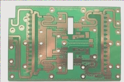
- Circuit Layer Design: Incorporate a grid pattern with a grid space of 10×10 mils, ensuring proper spacing and width for optimal material use.
- NPTH Hole Distance: Keep a distance of 20 mils between the NPTH hole and copper.
- Boards Formed by Milling: Maintain a distance of 16 mils between copper and the forming line, with similar spacing requirements for traces and frame.
- Die-Punched Boards: Ensure a distance of 20 mils between copper and the molding line for potential cost-saving mold opening in mass production.
- V-CUT Design: Design V-CUT lines based on board thickness to avoid issues, with specific distance requirements outlined for different thickness ranges.
Optimizing PCB layout is crucial for efficient manufacturing. Proper design considerations not only enhance production quality but also contribute to the overall performance and reliability of the final product.
One essential aspect to highlight is the use of grid-like copper patterns in circuit layers. While these patterns offer advantages in thermal performance and high-frequency conductivity, designers must also be mindful of potential issues related to heat dissipation and PCB deformation.
When designing PCB layouts, adherence to specific guidelines, such as maintaining adequate distances between components and copper elements, can significantly impact the functionality and longevity of the circuit board.