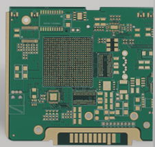
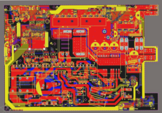
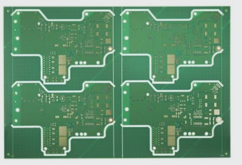
This article will delve into seven essential (and critical) skills and strategies for both novice and experienced printed circuit board (PCB) designers. By focusing on these skills throughout the PCB design process, you and your team can minimize redesign times, shorten overall design duration, and simplify the task of evaluating the final design results. Let’s examine each of these skills one by one.
1. Understand the PCB Manufacturing Process
In today’s fabless IC industry, many engineers may not fully grasp the steps involved in PCB production or the chemical treatments applied to their design files; this is not uncommon. However, this lack of practical understanding often leads novice engineers to make unnecessarily complex design choices.
Is the design truly required to be that intricate? Could using a larger grid for routing reduce circuit board costs and enhance reliability? Other common pitfalls for novice PCB designers include overly small via sizes, blind vias, and buried vias. While advanced through-hole structures can be valuable tools for PCB designers, their effectiveness is highly situational. Although these methods can be beneficial, they are not mandatory for every design.

2. The circuit diagram can simplify the design task
Sometimes, creating a simple circuit board and drawing schematics may seem like a waste of time, especially for those with prior design experience. However, for first-time PCB designers, crafting circuit diagrams can be quite challenging. Skipping the circuit diagram is a common strategy among novices and moderately experienced engineers, but it’s essential to develop your wiring based on a complete circuit diagram that serves as a reference to ensure accurate connections. Here’s why.
First, the circuit diagram visually represents the PCB circuit, conveying multiple levels of information; sub-areas of the circuit are detailed across several pages, with functionally related components positioned close together, independent of the final layout. Second, the circuit diagram’s symbols label each component’s pins, making it easy to identify any unconnected pins. In essence, whether or not you adhere to formal circuit rules, the diagram helps you quickly visualize and ensure circuit integrity.
When designing the PCB, having a circuit diagram as a template can simplify the wiring process. Utilizing circuit diagram symbols to establish connections allows you to tackle wiring challenges without overthinking them, ultimately reducing rework by catching missed connections in the first revision.
3. Use automatic routers, but don’t rely on them
Most professional PCB CAD tools include automatic routers, but unless you’re designing the PCB at a high level, these routers are typically only useful for preliminary designs; they do not provide a one-click solution for finalizing circuit links. You should still know how to wire manually.
When considering an auto-router, ask yourself: “After setting the constraints for the board and each trace on the circuit diagram, how much time do I have for manual wiring?” Experienced design engineers often dedicate most of their energy to initial layout, with nearly half of the design time spent optimizing component placement based on three key aspects:
– Simplified wiring—minimizing flying wire crossings.
– Proximity of components—shorter paths are better.
– Signal timing considerations.
4. Consider board size and current
Most individuals in electronic design understand that, like a river navigating a landscape, flowing electrons can encounter constrictions and bottlenecks; this concept directly applies to automotive fuse design. By controlling trace thickness and shape (U-bends, V-bends, S-bends, etc.), the fuse can be calibrated to blow at critical points when current overload occurs.
5. Avoid the risk of splinters
Slivers represent manufacturing errors that can be effectively managed through proper circuit board design. To grasp the sliver issue, we must review the chemical etching process. This process removes unnecessary copper, but if the etched area is particularly long and thin, fragments may detach before complete decomposition, floating in the chemical solution and potentially landing on another circuit board.
In this scenario, narrow shields between traces enhance the safety of the circuit board. There’s also a risk that slivers may remain on the original board; if narrow enough, the acid pool might corrode enough copper beneath to detach the sliver. Consequently, slivers can cling to the board and lead to shorts between traces.
6. Follow DRC
The auto-router settings typically align with design functionality, while the Design Rule Checker (DRC) captures manufacturer design constraints. Although setting up DRC can be tedious, it is more beneficial than relying solely on the auto-router. Most design teams establish a set of design rules aimed at standardizing production costs, maximizing yield, and ensuring consistency in assembly, inspection, and testing.
To address these challenges, many PCB design tools incorporate built-in DRCs—some refer to them as “constraint managers.” As you edit, the DRC will interactively highlight design violations; once you’ve set the DRC rules for your chosen manufacturer, be prepared to take any mistakes seriously.
7. Get to know existing foundry partners
After discussing DRC settings, this final PCB design tip may seem somewhat superfluous; however, it’s crucial for ensuring your circuit board design is manufacturable. Familiarizing yourself with your foundry partners can provide valuable pre-entry assistance.
—
Let me know if you need anything else!
1. Understand the PCB Manufacturing Process
In today’s fabless IC industry, many engineers may not fully grasp the steps involved in PCB production or the chemical treatments applied to their design files; this is not uncommon. However, this lack of practical understanding often leads novice engineers to make unnecessarily complex design choices.
Is the design truly required to be that intricate? Could using a larger grid for routing reduce circuit board costs and enhance reliability? Other common pitfalls for novice PCB designers include overly small via sizes, blind vias, and buried vias. While advanced through-hole structures can be valuable tools for PCB designers, their effectiveness is highly situational. Although these methods can be beneficial, they are not mandatory for every design.

2. The circuit diagram can simplify the design task
Sometimes, creating a simple circuit board and drawing schematics may seem like a waste of time, especially for those with prior design experience. However, for first-time PCB designers, crafting circuit diagrams can be quite challenging. Skipping the circuit diagram is a common strategy among novices and moderately experienced engineers, but it’s essential to develop your wiring based on a complete circuit diagram that serves as a reference to ensure accurate connections. Here’s why.
First, the circuit diagram visually represents the PCB circuit, conveying multiple levels of information; sub-areas of the circuit are detailed across several pages, with functionally related components positioned close together, independent of the final layout. Second, the circuit diagram’s symbols label each component’s pins, making it easy to identify any unconnected pins. In essence, whether or not you adhere to formal circuit rules, the diagram helps you quickly visualize and ensure circuit integrity.
When designing the PCB, having a circuit diagram as a template can simplify the wiring process. Utilizing circuit diagram symbols to establish connections allows you to tackle wiring challenges without overthinking them, ultimately reducing rework by catching missed connections in the first revision.
3. Use automatic routers, but don’t rely on them
Most professional PCB CAD tools include automatic routers, but unless you’re designing the PCB at a high level, these routers are typically only useful for preliminary designs; they do not provide a one-click solution for finalizing circuit links. You should still know how to wire manually.
When considering an auto-router, ask yourself: “After setting the constraints for the board and each trace on the circuit diagram, how much time do I have for manual wiring?” Experienced design engineers often dedicate most of their energy to initial layout, with nearly half of the design time spent optimizing component placement based on three key aspects:
– Simplified wiring—minimizing flying wire crossings.
– Proximity of components—shorter paths are better.
– Signal timing considerations.
4. Consider board size and current
Most individuals in electronic design understand that, like a river navigating a landscape, flowing electrons can encounter constrictions and bottlenecks; this concept directly applies to automotive fuse design. By controlling trace thickness and shape (U-bends, V-bends, S-bends, etc.), the fuse can be calibrated to blow at critical points when current overload occurs.
5. Avoid the risk of splinters
Slivers represent manufacturing errors that can be effectively managed through proper circuit board design. To grasp the sliver issue, we must review the chemical etching process. This process removes unnecessary copper, but if the etched area is particularly long and thin, fragments may detach before complete decomposition, floating in the chemical solution and potentially landing on another circuit board.
In this scenario, narrow shields between traces enhance the safety of the circuit board. There’s also a risk that slivers may remain on the original board; if narrow enough, the acid pool might corrode enough copper beneath to detach the sliver. Consequently, slivers can cling to the board and lead to shorts between traces.
6. Follow DRC
The auto-router settings typically align with design functionality, while the Design Rule Checker (DRC) captures manufacturer design constraints. Although setting up DRC can be tedious, it is more beneficial than relying solely on the auto-router. Most design teams establish a set of design rules aimed at standardizing production costs, maximizing yield, and ensuring consistency in assembly, inspection, and testing.
To address these challenges, many PCB design tools incorporate built-in DRCs—some refer to them as “constraint managers.” As you edit, the DRC will interactively highlight design violations; once you’ve set the DRC rules for your chosen manufacturer, be prepared to take any mistakes seriously.
7. Get to know existing foundry partners
After discussing DRC settings, this final PCB design tip may seem somewhat superfluous; however, it’s crucial for ensuring your circuit board design is manufacturable. Familiarizing yourself with your foundry partners can provide valuable pre-entry assistance.
—
Let me know if you need anything else!


