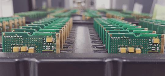
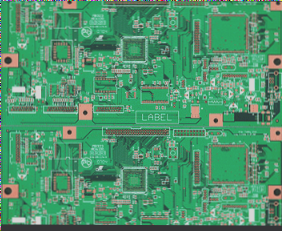
PCB Best Practices for Component Libraries, Layout, and Wiring
Component Library Requirements:
- Ensure accurate component package details, including pin dimensions and spacing.
- Clearly mark positive/negative poles for polar components in the library and on the PCB.
- Match pin numbers in the library with those in the schematic for consistency.
- Include heat sink dimensions for components needing heat dissipation.

Component Layout Guidelines:
- Arrange components uniformly, grouping functionally related ones together.
- Group components with the same power supply/ground network for better connectivity.
- Place interface components at the board edge and direct wiring away from the board.
- Provide ample space for heat dissipation for power conversion components.
PCB Wiring Standards:
- Isolate power supplies of different voltage levels to prevent crossing.
- Avoid sharp angles in wiring by using 45° or curved corners.
- Connect traces directly to the center of pads and maintain appropriate trace widths.
- Thicken power and ground lines for better current flow.
- Avoid routing traces beneath interference sources to minimize signal interference.
Additional Recommendations:
- Perform a Design Rule Check (DRC) to validate the design.
- Ensure correct placement of metal shell devices and module grounding.
- Position mounting pads appropriately for soldering.
- Apply teardrops to pads after wiring for better reliability.
PCB Delamination Considerations
Best Practices for PCB Layout
- The power plane should be positioned directly beneath the ground plane and tightly coupled with it to optimize performance.
- Signal layers need to be placed next to inner electrical layers, avoiding direct adjacency with other signal layers for improved signal integrity.
- Isolate digital and analog circuits whenever possible. Consider placing them on separate layers with proper shielding. If they must share a layer, use isolation bands and ground lines to minimize interference. Keep analog and digital power supplies and grounds separate.
- For high-frequency circuits susceptible to external interference, separate them from other components. Utilize intermediate signal layers adjacent to inner electrical layers to take advantage of the copper film and reduce external interference.
Latest PCB Layout Trends
Recent advancements in PCB design focus on enhancing signal integrity and reducing interference. Incorporating advanced simulation tools can help predict and mitigate signal integrity issues early in the design phase. Additionally, the rise of flexible and rigid-flex PCBs offers more design flexibility for complex applications.