Effective PCB Design Tips for Efficient Assembly
Understanding PCB Design for Assembly (DFA)
PCB assembly involves integrating the circuit board with electronic components to create the final product. PCB assembly design focuses on optimizing the assembly process during the early design phase.
- One common issue is neglecting assembly considerations during initial PCB design, leading to future problems.
- Component placement and spacing are crucial to prevent assembly complications and ensure product performance.
Issues such as component availability can disrupt the manufacturing process if not addressed early.
Key Tips for PCB Assembly Design
1. Ensure Proper Component Spacing
Improper spacing between components can result in redesigns and increased costs. Creating adequate spacing using techniques like place_boundary in Allegro can prevent assembly issues.
Engineers must avoid overlapping place_boundary shapes for components to maintain proper spacing.
Minimum spacing requirements vary based on component types, with capacitors and resistors requiring at least 10 mils of spacing.
2. Early Component Selection
Selecting components early helps prevent conflicts between design and assembly processes. Collaboration between engineers can optimize component sizes for efficient PCB assembly.
3. Segregate Leaded and Lead-Free Components
Separating lead-free and leaded components during assembly is crucial to maintain solder quality and comply with environmental standards.
4. Ensure Even Placement of Large Components
Even distribution of large components aids in uniform heat distribution during solder reflow. Customizing heat profiles for reflow ovens enhances the assembly process.
5. Opt for Suitable Footprint Sizes
Choosing appropriate footprint sizes is essential for efficient PCB assembly and overall product performance.
PCB Layout Best Practices
When designing a PCB layout, it is crucial to consider various factors to ensure efficient assembly and manufacturing processes. Here are some key tips to optimize your PCB design:
1. Opt for Larger Components When Possible
During the layout phase, consider using larger components like 0402 resistors instead of smaller ones like 0201 resistors. Choosing suitable component sizes can enhance assembly efficiency and prevent unnecessary PCB size increase.
2. Avoid Mixed Manufacturing Processes
Avoid mixing manufacturing processes whenever feasible. It is more efficient to use either all through-hole components or none at all. Placing all through-hole components on one side of the board can streamline production.
3. Check Component Lead Times
Verify the availability of components before starting the design to prevent delays. Place advance orders for components with long lead times to ensure timely delivery of the final product.
4. Keep the Bill of Materials (BOM) Updated
Regularly review and update the BOM to avoid assembly delays. Ensure that the BOM includes accurate part numbers, descriptions, and component values.
5. Verify Component Footprints
Accurately create component footprints based on datasheet pad patterns. Misinterpreting datasheet guidelines can lead to design errors and necessitate board redesign. Refer to our guide for creating footprints in Allegro for more information.
6. Include Instructional Markings
Ensure all essential markings like Pin1 indicators, component polarity, and orientation are present on the silkscreen layer to avoid assembly issues.
Remember, a well-planned PCB layout can significantly impact the efficiency and quality of your final product.
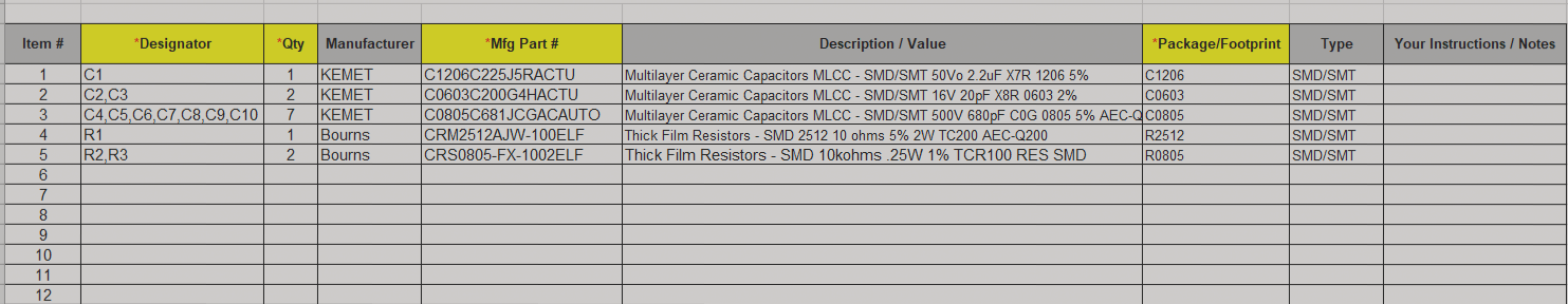
Additional useful information to include in your BOM:
- Quantity per PCB
- Distributor Name
- Distributor Part Number