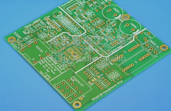
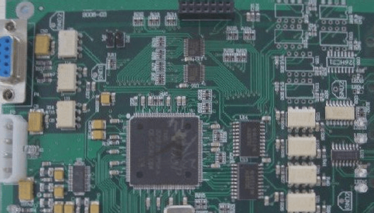
Nowadays, the factors considered in PCB board design are increasingly complex, such as clocking, crosstalk, impedance, detection, and manufacturing processes. These complexities often require designers to repeat extensive layout, verification, and maintenance work. The Parameter Constraint Editor can systematize these parameters to help designers effectively manage these sometimes conflicting factors during the design and production phases.
In recent years, demands for PCB board layout and wiring have grown more intricate. Integrated circuits continue to escalate in transistor count as predicted by Moore’s Law, enhancing device speed and shortening the rise time of each pulse edge. Concurrently, the number of pins per device is also rising, often reaching 500 to 2,000 pins. These advancements contribute to issues like density, clocking, and crosstalk in PCB design.
A few years ago, most PCB boards featured only a handful of “critical” nodes (nets), typically constrained by factors such as impedance, trace length, and clearance. Designers typically addressed these traces manually before employing software for automated circuit-wide routing. Today, PCBs commonly feature 5,000 or more nodes, with over 50% categorized as critical. Time-to-market pressures have rendered manual routing impractical. Moreover, not only has the number of critical nodes increased, but so have the constraints on each node. These constraints stem largely from parameter interdependencies and increasingly sophisticated design requirements.
For instance, the spacing between two traces may hinge on factors such as node voltage and board material characteristics. The decreasing rise times of digital ICs impact both high and low-speed designs, influencing setup and hold times due to accelerated pulse generation. Interconnect delay now significantly contributes to total delay in high-speed circuit designs, and remains crucial even in low-speed applications.
Addressing these challenges would be easier with larger board designs, yet the prevailing trend favors miniaturization. Interconnect delays and high-density packaging requirements are shrinking circuit boards, necessitating adherence to stringent miniaturization guidelines. This trend, combined with reduced rise times, exacerbates issues like crosstalk noise. High-density packages such as ball grid arrays can further intensify problems like crosstalk, switching noise, and ground bounce.

Fixed constraints exist. The traditional approach to addressing these issues involves translating electrical and process requirements into fixed constraint parameters using experience, default values, tables, or calculations. For instance, in circuit design, an engineer might first establish a target impedance and then “estimate” a suitable trace width to achieve the required impedance based on process requirements. Alternatively, they might use calculation tables or software tools to assess interference and derive length constraints. This methodology typically necessitates establishing a set of empirical data as foundational guidelines for PCB designers, which can be applied alongside automated place-and-route tools.
The drawback of this approach lies in the fact that empirical data serves as a general guideline and, although mostly accurate, can occasionally fail or yield incorrect results. Let’s consider the example of impedance determination mentioned earlier to illustrate potential errors stemming from this method. Factors influencing impedance include the dielectric properties of circuit board materials, the thickness of copper foils, the spacing between each layer and the ground/power layer, and the trace width. Since the first three parameters are usually dictated by the manufacturing process, designers typically rely on trace width to control impedance. However, since each circuit layer may differ in its proximity to the ground or power layer, applying uniform empirical data across all layers can lead to inaccuracies. Moreover, changes in production processes or board characteristics during development can further complicate matters. Often, such issues surface during prototyping stages, necessitating costly circuit board repairs or redesigns upon their discovery. These fixes often introduce additional complications requiring further debugging, while delays in time-to-market can lead to substantial revenue losses far surpassing debugging costs. Nearly every electronics manufacturer grapples with these challenges, highlighting that conventional PCB design software fails to keep pace with contemporary electrical performance requirements, unlike its mechanical design counterparts.
**Solution: Parametric Constraints**
In response, design software vendors are now addressing these issues by introducing parametric constraints. This approach enables the specification of mechanical specifications that fully capture internal electrical characteristics. Once incorporated into PCB designs, this information empowers design software to control automated placement and routing tools. When subsequent changes occur in the production process, there’s no need for redesigns. Designers simply update process characteristic parameters to automatically adjust relevant constraints. Subsequently, designers can conduct Design Rule Checks (DRC) to identify violations of other design rules and pinpoint necessary design adjustments to rectify errors.
Constraints can be input as mathematical expressions encompassing constants, various operators, vectors, and other design constraints. They can also be stored in design files or schematics as lookup tables. PCB routing, copper foil positioning, and layout tools must adhere to constraints derived from these conditions. DRC verifies overall compliance with these constraints, encompassing trace width, spacing, spatial requirements (such as area and height constraints), and more.
**Hierarchical Management:**
A significant advantage of parametric constraints lies in their hierarchical manageability. For instance, a global trace width rule can serve as a design constraint across the entire design. However, specific regions or nodes may necessitate deviating from this principle. In such cases, hierarchical designs enable overriding higher-level constraints in favor of lower-level ones tailored to specific nodes or regions.
1) Design constraints apply universally across all objects without exceptions.
2) Hierarchical constraints pertain to objects on specific layers.
3) Node-type constraints affect all nodes of a certain type.
4) Node constraints are specific to individual nodes.
5) Inter-class constraints govern relationships between two node types.
6) Space constraints apply to all devices within a designated area.
7) Device constraints are specific to particular devices.
**Example 1: Line Width = f (Impedance, Layer Spacing, Dielectric Constant, Copper Foil Height)**
Consider how parametric constraints serve as design rules for controlling impedance. Given a predetermined impedance requirement, parameters such as dielectric constant, spacing from nearby layers, and copper foil height can be treated as variables within the impedance formula. Typically, the trace width is the sole parameter designers can adjust. Therefore, constraints on trace width are defined as functions of impedance, dielectric constant, layer spacing, and copper foil height. By setting these formulas as level constraints and incorporating manufacturing process parameters as design-level constraints, software can automatically adjust trace widths to accommodate changes in layer stacking during design iterations. Similarly, changes in copper foil height due to shifts in manufacturing processes only necessitate updating the corresponding parameter at the design level, thereby triggering automatic recalculation of relevant constraints.
**Example 2: Device Spacing = max(Default Spacing, f(Device Height, Inspection Angle))**
Parametric constraints combined with Design Rule Checking (DRC) enhance the portability and traceability of design modifications. For instance, device spacing can be determined by process parameters and testing requirements. The formula indicates that device spacing is a function of device height and inspection angle. Since inspection angles typically remain constant across the board, they are defined at the design level. Updating these parameters in response to shifts in testing equipment can be swiftly verified using DRC to ensure the revised spacing aligns with new specifications, simplifying the design process compared to manual recalculations.
**Example 3: Component Layout**
Design rules also govern component placement, ensuring devices are positioned according to constraints without introducing errors. Figure 1 highlights device placement areas compliant with physical constraints (e.g., spacing from board edges, device spacing), while Figure 2 showcases areas satisfying electrical constraints like trace lengths. Figure 3 depicts areas meeting spatial constraints exclusively, with Figure 4 representing the intersection of these areas—designating the effective layout zone where devices meet all stipulated constraints.
By structuring constraints in a modular fashion, their maintainability and reusability are significantly enhanced. New expressions can reference constraint parameters from prior stages, such as the top layer trace width depending on top-layer distances, copper line heights, and variables like Temp and Dielectric Constant at the design level. Note that constraints are displayed in ascending order, with adjustments to higher-level constraints immediately influencing all lower-level expressions referencing them.
**Design Reuse and Documentation**
Parametric constraints not only streamline initial design processes but also facilitate subsequent engineering changes and design reuse. These constraints become integral components of design systems and documentation, ensuring continuity and fidelity to original design intent. Future users can readily access and modify design rules based on updated process requirements without the guesswork associated with legacy practices.
The Parametric Constraint Editor simplifies PCB layout and routing under multi-dimensional constraints, enabling automated routing software to comprehensively validate designs against complex electrical and process requirements. This approach ultimately yields successful PCB designs, potentially reducing or eliminating the need for prototyping altogether.


