With the rapid advancement of high-performance electronic devices and equipment, the electronics industry has experienced significant global growth. Electronic innovation is thriving across various sectors, including automotive, military, aerospace, defense, marine, telecommunications, and many others. A critical component in modern electronic equipment is high-density interconnect (HDI) technology, which is used to design and build printed circuit boards (PCBs). HDI PCBs facilitate electrical connectivity between different layers via small and precise vias, controlled through drilling processes. Drilling is therefore crucial in both the design and manufacturing stages of PCB production. This article provides an overview of drilling technology in PCB manufacturing, focusing on the latest trends and developments.
### Introduction to Drilling Machines and Drilling Technology
In the past, PCB drilling was performed using simple, manual drilling machines. Operators would move the panels by hand to adjust the x and y coordinates, and manually operate the lever to create holes, a process that was both time-consuming and labor-intensive. However, with technological advancements, PCB drilling has evolved significantly. Today’s advanced drilling machines are capable of producing boards with more than 10,000 holes of varying sizes, all with high precision. The shift from manual to automated systems has greatly enhanced production efficiency and accuracy, driving the growth of the electronics market.
### Evolution of PCB Drilling Techniques
Modern PCB drilling machines are equipped with computer numerical control (CNC) systems, which allow for precise positioning and rapid drilling of holes in multiple layers of the circuit board. This automation not only speeds up the manufacturing process but also minimizes human error, improving overall quality and reliability. The ability to drill microvias and fine holes with tight tolerances has become essential for HDI boards, which require more advanced techniques than traditional PCBs.
### Current Trends in Drilling Technology
Several key trends are shaping the future of PCB drilling technology:
1. **Miniaturization**: As devices continue to become smaller and more powerful, there is a growing demand for PCBs with tighter component spacing and smaller vias. New drilling technologies, such as laser drilling and fine-pitch mechanical drilling, are being developed to meet these needs.
2. **Laser Drilling**: Laser drilling has become a popular choice for creating microvias in HDI boards due to its ability to achieve high precision with minimal damage to surrounding areas. This non-contact method offers greater flexibility and efficiency, particularly for complex designs with dense interconnections.
3. **Automation and Smart Systems**: Automated drilling systems integrated with real-time monitoring and adaptive feedback mechanisms are becoming more common. These systems not only improve speed but also enhance the quality control process, ensuring that each hole meets the required specifications.
4. **Material Considerations**: The materials used for PCBs are also evolving. As new materials with higher thermal and electrical performance are introduced, they often require specialized drilling techniques to maintain the integrity of the board.
### Conclusion
PCB drilling is a fundamental aspect of circuit board manufacturing, playing a crucial role in creating high-density, high-performance electronics. As the demand for smaller, more complex designs grows, advanced drilling technologies such as laser drilling and automated systems are becoming increasingly important. The ongoing evolution of PCB drilling techniques will continue to drive innovation across various industries, supporting the development of next-generation electronic devices.

### Drilling in PCB Manufacturing: Techniques and Best Practices
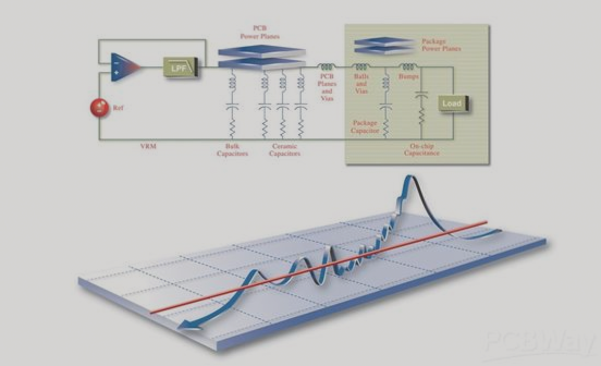
Drilling is a crucial process in PCB manufacturing, typically performed to create holes that connect the different layers of a circuit board both electrically and thermally. These holes are known as **vias** when used to interconnect layers. The primary purpose of drilling in PCB fabrication is to allow the insertion of through-hole component leads or establish electrical connections between the layers, ensuring the creation of a functional circuit. The drilling process is a critical part of PCB design and manufacturing, influencing the layout, material selection, manufacturing method, and choice of via types. A misstep in drilling can be costly, as it can lead to trace damage, affecting the circuit’s performance and potentially resulting in production defects that waste materials.
### Drilling Machines and Technology Evolution
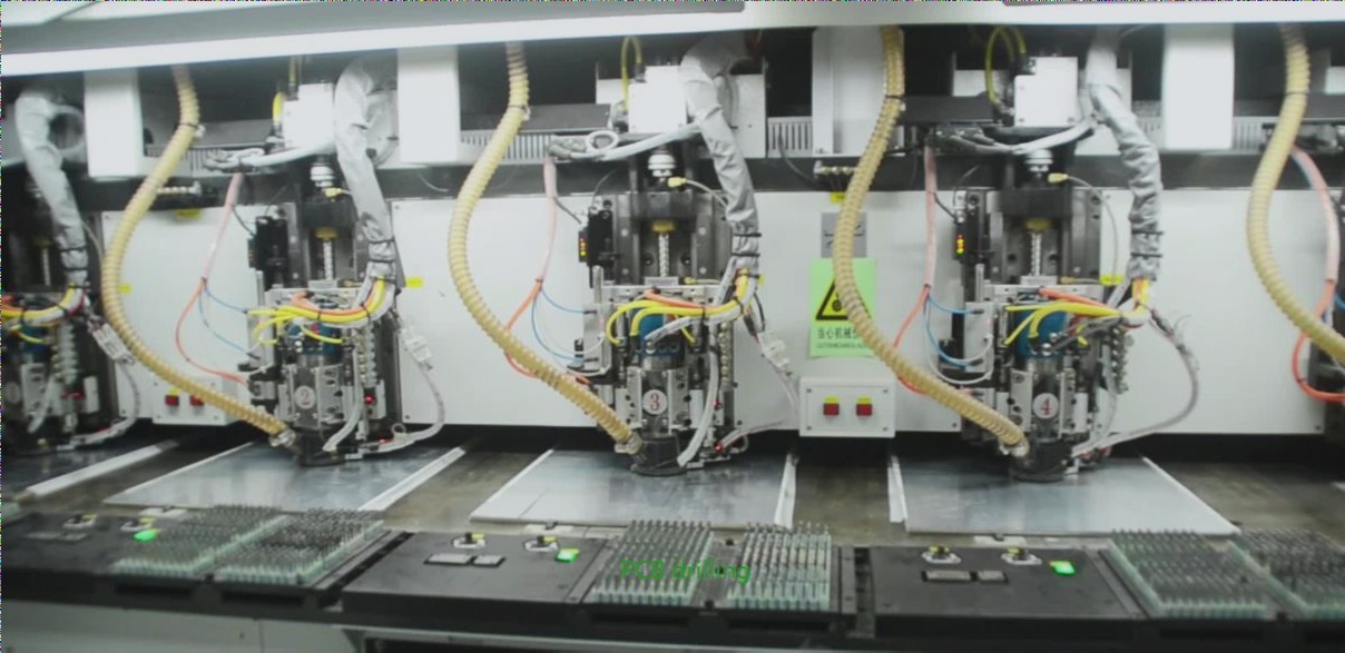
PCB drilling has evolved significantly due to technological advancements. Modern drilling operations are performed using various specialized machines such as small-diameter drills, automatic drilling machines, CNC (Computer Numerical Control) machines, and other highly effective equipment, all suited for different types of circuit boards.
Automatic drilling machines are controlled by computers, enabling precise hole creation with minimal human intervention. CNC machines are particularly advantageous when drilling multiple holes of different sizes, as they offer high precision and can reduce production time and costs.
In cases where registered holes are required, additional accuracy is necessary. For such applications, **X-ray drilling** is employed, which ensures that the drill precisely targets the center of the inner pad. This technique is commonly used when through-holes connect copper layers or are drilled to accommodate lead components.
### Innovations in Drilling: Laser Technology and Micro-Vias
For drilling smaller holes, traditional mechanical drills may cause damage to the PCB and increase costs. To address this issue, **laser drilling** technology has emerged as a more accurate solution. Laser drilling allows for the creation of **micro-vias**, which are tiny holes used for layer interconnection in PCBs. One widely adopted laser technology is **CO2 laser drilling**, which is used for creating inner through-holes. This method ensures precision without compromising the integrity of the PCB, especially when dealing with fine-pitch designs and high-density interconnects (HDI).
If the goal is to connect only certain copper layers without passing through the entire PCB, **depth-controlled drilling** or pre-drilling before PCB lamination or laser drilling can be used. This helps in controlling the drilling depth and ensures the correct connection between layers without drilling through the entire board.
### Early Stage PCB Planning: The Importance of Expert Consultation
It is highly recommended to involve **PCB drilling experts** early in the PCB design process. Their expertise can help define the optimal PCB layout and determine the most suitable drilling techniques and materials. Proper consultation at this stage will ensure that the drilling process is efficient and the PCB design is feasible within production constraints.
### Cost Reduction through Precise Drilling
Precision in the drilling process plays a significant role in reducing production costs. Drilling at the optimal speed not only minimizes the time spent but also reduces tool wear and prevents breakage, which can lead to costly rework. Proper control of drilling speed, tool size, and plate thickness can result in significant cost savings by optimizing the material usage and reducing the chances of defects.
Moreover, maintaining a balance between speed and precision is critical. Too fast a drilling speed may lead to tool failure, while too slow could result in increased time and energy consumption. Hence, effective management of drilling parameters, including drill bit size and material thickness, can help streamline production and lower costs.
### Conclusion: Achieving Efficient Drilling for Optimal PCB Performance
In conclusion, while reducing drilling costs is essential, it is equally important to ensure that the **electrical conductivity** between layers is uninterrupted and that the component installation is efficient. By focusing on precision and integrating advanced drilling techniques like laser drilling for micro-vias, manufacturers can maintain high-quality standards and cost-efficiency. As PCB technology advances, a balanced approach to drilling operations, including the use of automated tools and expert guidance during the early stages of design, will continue to be crucial for achieving both cost-effective and reliable PCBs.
### Introduction to Drilling Machines and Drilling Technology
In the past, PCB drilling was performed using simple, manual drilling machines. Operators would move the panels by hand to adjust the x and y coordinates, and manually operate the lever to create holes, a process that was both time-consuming and labor-intensive. However, with technological advancements, PCB drilling has evolved significantly. Today’s advanced drilling machines are capable of producing boards with more than 10,000 holes of varying sizes, all with high precision. The shift from manual to automated systems has greatly enhanced production efficiency and accuracy, driving the growth of the electronics market.
### Evolution of PCB Drilling Techniques
Modern PCB drilling machines are equipped with computer numerical control (CNC) systems, which allow for precise positioning and rapid drilling of holes in multiple layers of the circuit board. This automation not only speeds up the manufacturing process but also minimizes human error, improving overall quality and reliability. The ability to drill microvias and fine holes with tight tolerances has become essential for HDI boards, which require more advanced techniques than traditional PCBs.
### Current Trends in Drilling Technology
Several key trends are shaping the future of PCB drilling technology:
1. **Miniaturization**: As devices continue to become smaller and more powerful, there is a growing demand for PCBs with tighter component spacing and smaller vias. New drilling technologies, such as laser drilling and fine-pitch mechanical drilling, are being developed to meet these needs.
2. **Laser Drilling**: Laser drilling has become a popular choice for creating microvias in HDI boards due to its ability to achieve high precision with minimal damage to surrounding areas. This non-contact method offers greater flexibility and efficiency, particularly for complex designs with dense interconnections.
3. **Automation and Smart Systems**: Automated drilling systems integrated with real-time monitoring and adaptive feedback mechanisms are becoming more common. These systems not only improve speed but also enhance the quality control process, ensuring that each hole meets the required specifications.
4. **Material Considerations**: The materials used for PCBs are also evolving. As new materials with higher thermal and electrical performance are introduced, they often require specialized drilling techniques to maintain the integrity of the board.
### Conclusion
PCB drilling is a fundamental aspect of circuit board manufacturing, playing a crucial role in creating high-density, high-performance electronics. As the demand for smaller, more complex designs grows, advanced drilling technologies such as laser drilling and automated systems are becoming increasingly important. The ongoing evolution of PCB drilling techniques will continue to drive innovation across various industries, supporting the development of next-generation electronic devices.
### Drilling in PCB Manufacturing: Techniques and Best Practices
Drilling is a crucial process in PCB manufacturing, typically performed to create holes that connect the different layers of a circuit board both electrically and thermally. These holes are known as **vias** when used to interconnect layers. The primary purpose of drilling in PCB fabrication is to allow the insertion of through-hole component leads or establish electrical connections between the layers, ensuring the creation of a functional circuit. The drilling process is a critical part of PCB design and manufacturing, influencing the layout, material selection, manufacturing method, and choice of via types. A misstep in drilling can be costly, as it can lead to trace damage, affecting the circuit’s performance and potentially resulting in production defects that waste materials.
### Drilling Machines and Technology Evolution
PCB drilling has evolved significantly due to technological advancements. Modern drilling operations are performed using various specialized machines such as small-diameter drills, automatic drilling machines, CNC (Computer Numerical Control) machines, and other highly effective equipment, all suited for different types of circuit boards.
Automatic drilling machines are controlled by computers, enabling precise hole creation with minimal human intervention. CNC machines are particularly advantageous when drilling multiple holes of different sizes, as they offer high precision and can reduce production time and costs.
In cases where registered holes are required, additional accuracy is necessary. For such applications, **X-ray drilling** is employed, which ensures that the drill precisely targets the center of the inner pad. This technique is commonly used when through-holes connect copper layers or are drilled to accommodate lead components.
### Innovations in Drilling: Laser Technology and Micro-Vias
For drilling smaller holes, traditional mechanical drills may cause damage to the PCB and increase costs. To address this issue, **laser drilling** technology has emerged as a more accurate solution. Laser drilling allows for the creation of **micro-vias**, which are tiny holes used for layer interconnection in PCBs. One widely adopted laser technology is **CO2 laser drilling**, which is used for creating inner through-holes. This method ensures precision without compromising the integrity of the PCB, especially when dealing with fine-pitch designs and high-density interconnects (HDI).
If the goal is to connect only certain copper layers without passing through the entire PCB, **depth-controlled drilling** or pre-drilling before PCB lamination or laser drilling can be used. This helps in controlling the drilling depth and ensures the correct connection between layers without drilling through the entire board.
### Early Stage PCB Planning: The Importance of Expert Consultation
It is highly recommended to involve **PCB drilling experts** early in the PCB design process. Their expertise can help define the optimal PCB layout and determine the most suitable drilling techniques and materials. Proper consultation at this stage will ensure that the drilling process is efficient and the PCB design is feasible within production constraints.
### Cost Reduction through Precise Drilling
Precision in the drilling process plays a significant role in reducing production costs. Drilling at the optimal speed not only minimizes the time spent but also reduces tool wear and prevents breakage, which can lead to costly rework. Proper control of drilling speed, tool size, and plate thickness can result in significant cost savings by optimizing the material usage and reducing the chances of defects.
Moreover, maintaining a balance between speed and precision is critical. Too fast a drilling speed may lead to tool failure, while too slow could result in increased time and energy consumption. Hence, effective management of drilling parameters, including drill bit size and material thickness, can help streamline production and lower costs.
### Conclusion: Achieving Efficient Drilling for Optimal PCB Performance
In conclusion, while reducing drilling costs is essential, it is equally important to ensure that the **electrical conductivity** between layers is uninterrupted and that the component installation is efficient. By focusing on precision and integrating advanced drilling techniques like laser drilling for micro-vias, manufacturers can maintain high-quality standards and cost-efficiency. As PCB technology advances, a balanced approach to drilling operations, including the use of automated tools and expert guidance during the early stages of design, will continue to be crucial for achieving both cost-effective and reliable PCBs.