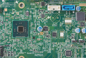
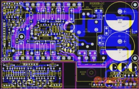
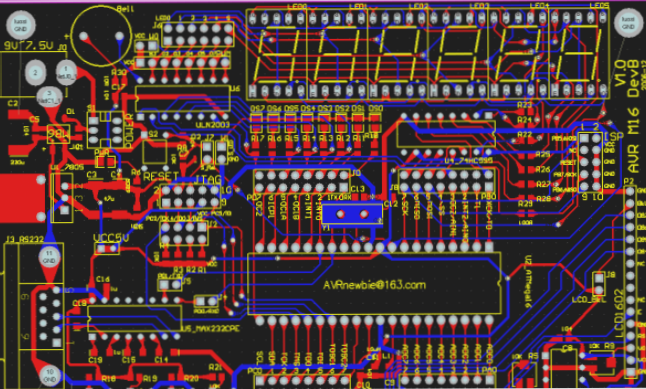
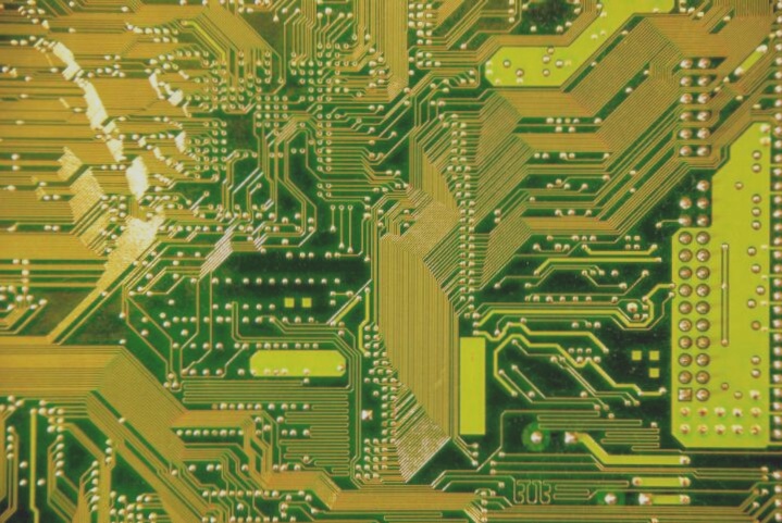
1. Printed circuit boards serve as the foundation for circuit components and devices in electronic products. They provide essential electrical connections between circuit components and are fundamental to all electronic devices. With the widespread use of large and very large scale integrated circuits in electronic equipment, the mounting density of components on printed circuit boards is increasing, and the signal transmission speed continues to rise. Consequently, the EMC issues related to these developments are becoming more significant.

2. Printed circuit boards are classified into single-sided (single-layer), double-sided (double-layer), and multilayer boards. Single and double-sided boards are typically used for low to medium density wiring and circuits with lower integration, while multilayer PCBs support high-density wiring and circuits with higher integration. Single and double-sided boards are unsuitable for high-speed circuits, as their wiring capabilities cannot meet the demands of high-performance systems. The advancement of multilayer wiring technology offers a solution to these limitations, and its application is becoming increasingly widespread.

3. Features of multilayer wiring.

Multilayer circuit boards are composed of both organic and inorganic dielectric materials, featuring a multi-layer structure. These layers are interconnected by vias. By plating or filling vias with metal, electrical signal conduction between layers can be achieved. Due to several advantageous characteristics, multilayer wiring has become widely adopted:

(1) Multilayer boards include dedicated power and ground layers. The power layer can act as a noise source to minimize interference, while simultaneously providing a path for all system signals, eliminating common impedance coupling interference. This reduces the impedance of the power supply line, thereby diminishing common impedance issues in the power system.

(2) Multilayer boards incorporate a dedicated ground layer, with all signal traces having their own specific ground connections. The design of these signal traces offers stable impedance, improved matching, and minimized waveform distortion caused by reflection. The dedicated ground layer increases distributed capacitance between the signal and ground traces, which helps reduce crosstalk.

4. Laminate design of the printed circuit board.

Wiring rules for PCB boards.

1. The electromagnetic compatibility (EMC) analysis of a multilayer PCB can be conducted using Kirchhoff’s law and Faraday’s law. According to Kirchhoff’s law, any signal traveling from the source to the load in the time domain must follow the path of lowest impedance.

2. Multilayer PCBs are commonly used in high-speed, high-performance systems, where they serve as reference planes for DC power or ground. These layers are typically not solid planes, as they are intended to handle multiple DC voltages and provide return paths for current in adjacent signal transmission lines. The primary objective in these designs is to establish low-impedance current loops for improved EMC performance.

3. The signal layers are positioned between the physical reference planes, and they may include either symmetrical or asymmetrical striplines. A 12-layer board serves as an example for explaining the structure and layout of multilayer PCBs. Its architecture follows the pattern T-P-S-P-S-P-B, where T represents the top layer, P is a reference plane, S is a signal layer, and B is the bottom layer. These layers are numbered 1 through 12, starting from the top. For components with upper and lower pads, long-distance signal transmission is avoided to reduce direct radiation from traces. It is also important to isolate incompatible signal lines to prevent coupling interference. High-frequency, low-frequency, high-current, and small-current signals, as well as digital and analog signals, should be kept separate. Proper component placement and signal isolation should be prioritized during layout.

4. Three key design considerations include:

– Selecting a reference layer to handle multiple DC voltage regions. If, for instance, the eleventh layer accommodates multiple DC voltages, the designer must place high-speed signals away from the tenth and bottom layers. This is because the loop current cannot pass through the reference plane above the tenth layer, requiring the use of stitching capacitors.

– The fifth, seventh, and ninth layers are designated for high-speed signals. Routing critical signals in a single direction on these layers helps to optimize routing space. Signal traces between layers should be kept perpendicular to each other to minimize electromagnetic interference. For example, the third and seventh layers can follow east-west routing, while the fifth and ninth layers can be oriented for south-north routing, depending on the destination of the signal.

– Managing layer transitions during high-speed signal routing to ensure the return current flows from one reference plane to another. This minimizes the signal loop area and reduces radiation from both differential-mode and common-mode currents. The radiation intensity of a loop is directly proportional to its area. Ideally, the reference plane should remain unchanged, with only one side needing adjustment for return current. Specific signal layer pairs (e.g., layers 3, 5, 7, 9) can be used for routing in both east-west and north-south orientations. However, pairing layers 3 and 9 is not ideal, as the return current must travel from layer 4 to layer 8, increasing the loop area.

5. When designing for decoupling capacitors, it is important to minimize via inductance, which can reduce their effectiveness at high frequencies. While decoupling capacitors should be placed near vias, their function is compromised by the inductive nature of vias, increasing the area of the signal loop and weakening current radiation.

6. For selecting the DC voltage reference layer, it is crucial to address the noise generated by high-speed processors, especially on power/ground reference pins. Efficient use of decoupling capacitors is essential, with the goal of minimizing the inductance of these components. This can be achieved by making the traces as short, wide, and direct as possible, and by using short, thick vias.

7. When the second layer is assigned as ground and the fourth layer as the processor power supply, vias should be kept as short as possible to minimize the distance between the processor and decoupling capacitors. There is no significant current flowing through the space extending to the bottom of the board, and this area will not function as an antenna when short-circuited. The reference configuration for cascading design layout is shown in Table 1.

8. **The 20-H Rule and 3-W Rule:**

There are two fundamental guidelines for determining the distance between power layers and edge boundaries, as well as the spacing between printed lines: the 20-H principle and the 3-W principle.

– **20-H Principle:** RF currents typically exist at the edge of the power plane due to magnetic flux interactions. When high-speed digital or clock signals are present, RF currents can couple with one another, as illustrated in Figure 1. To mitigate this effect, the physical size of the power plane should be at least 20 times the distance (H) smaller than the nearest ground plane. The edge effect of the power plane generally becomes significant at about 10H, with 20H reducing about 10% of the magnetic flux. To block up to 98% of the magnetic flux, a boundary of 100% is required, as shown in Figure 1. The 20-H rule governs the physical distance between the power plane and its nearest ground plane, including the thickness of copper-clad laminate and any insulating layers. Applying this rule increases the resonant frequency of the PCB.

– **3-W Principle:** When the distance between PCB traces is too small, electromagnetic crosstalk can occur, interfering with the normal operation of related circuits. To avoid this, the spacing between traces should be at least three times the trace width, i.e., no less than 3W (W being the trace width). Trace width is critical for line impedance requirements. If the trace is too wide, it affects the wiring density, while a trace that is too narrow impacts signal integrity and transmission strength. The 3-W rule applies to clock circuits, differential pairs, and I/O port wiring. It ensures that crosstalk energy is attenuated by at least 70%. For stricter requirements, a higher boundary can be specified to achieve 98% attenuation.

Leave a Comment

Contact

WellCircuits
More than PCB

Upload your GerberFile(7z,rar,zip)