The Intricacies of PCB Production Process
In the PCB industry, operations are driven by customer orders, often requiring adjustments throughout the production cycle. These adjustments, such as altering process routes to accommodate client demands, must be meticulously updated in the system. Additionally, production resources operate at predetermined scales, complicating planning and scheduling.
Materials and Processes
- Open Material: Copper sheets are cut into various sizes to create the PCB’s internal circuitry.
- Internal Printing: The inner layer of the circuit board is printed on copper sheets.
- Pressing: A protective layer is pressed onto the circuit board to prevent damage.
- Drilling: Holes are drilled in the board for component attachment.
- PTH: Copper is used in holes for durability.
- Outside Lines: Printing of the outer circuit board begins.
- Plating: Tin is applied and etched on the board.
- Half Test: Semi-finished products are tested for internal wiring issues.
- Solder Mask, Spray Tin, Text: Further processes in PCB production.
Quality Control and Monitoring
PCB production involves stringent quality control measures. The CheckPoint method allows for close monitoring at each stage to ensure timely delivery and product quality. Work in Progress (WIP) is closely tracked, with output measured in square feet.
Significance of PCBs
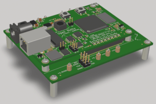
PCBs play a crucial role in modern electronics, serving as the foundation for various devices. Their production involves intricate processes to ensure functionality and reliability in electronic applications.

PCBs: A Fundamental Component in Electronics
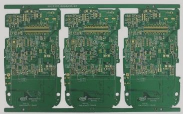
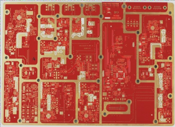
Printed circuit boards (PCBs) play a crucial role in the information and electronics industry, falling under the electronic component sector. They come in various types based on layers and flexibility.
Types of PCBs:
- Single-sided boards (SSB)
- Double-sided boards (DSB)
- Multi-layer boards (MLB)
Flexibility Categories:
- Rigid printed circuit boards (RPC)
- Flexible printed circuit boards (FPC)
The PCB industry is segmented into six main categories:
- Single-sided boards
- Double-sided boards
- Conventional multilayer boards
- Flexible boards
- HDI (high-density interconnect) boards
- Package substrates
Stay updated with the latest advancements in PCB technology to meet the evolving demands of the electronics market.


