1. Recently, I have been conducting ESD tests on electronic products, and the results have underscored the critical importance of this assessment. If a circuit board is inadequately designed, static electricity can lead to product crashes or component damage. While we previously recognized that ESD could harm components, we underestimated its significance in electronic product design.
2. ESD, or Electro-Static Discharge, is a natural phenomenon involving the generation of static electricity through contact, friction, or electrical induction. It typically accumulates over time, generating high voltages (thousands to tens of thousands of volts), low power, small currents, and brief durations of action. In electronic products, poorly designed ESD protection can result in unstable operation or outright damage.
3. ESD discharge testing employs two methods: contact discharge and air discharge. Contact discharge involves directly discharging test equipment, while air discharge, also known as indirect discharge, occurs due to the coupling of strong magnetic fields with adjacent current loops. Test voltages for these methods generally range from 2KV to 8KV, with specific requirements varying across regions. Therefore, market considerations are crucial in the design phase.
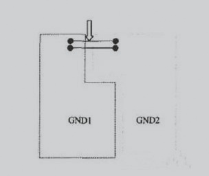
4. Electrostatic protection design typically involves three steps: preventing external charges from entering the circuit board and causing damage; shielding the board from external magnetic fields; and mitigating hazards from electrostatic fields.
5. In actual circuit design, various methods are employed for electrostatic protection:
6. Avalanche diode clamping is a common method, involving the connection of key signal lines to ground through avalanche diodes. These diodes respond quickly and provide stable clamping, dissipating accumulated high voltages to protect the circuit board.
7. Placing ceramic capacitors (rated at least 1.5 KV) in I/O connectors or critical signal positions, and minimizing cable length to reduce cable inductance, is effective. Using low voltage capacitors can lead to capacitor damage and loss of protection.
8. Ferroxide beads effectively attenuate ESD currents and suppress radiation, making them a suitable choice for addressing multiple issues simultaneously.
9. Tip discharge, implemented by aligning triangular copper sheets on microstrip layers, offers protection by generating tip discharges that dissipate static electricity.
10. LC filters effectively reduce high-frequency static electricity entering the circuit. Inductive properties suppress high-frequency ESD, while capacitance diverts energy to ground, enhancing signal integrity and reducing RF effects.
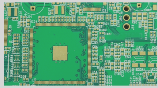
11. Utilizing multilayer boards, when feasible, is an effective means of ESD prevention, providing additional protection by coupling ESD to low impedance ground planes more rapidly.
12. Routing wires around the circuit board without additional solder layers helps prevent ESD.
13. When possible, connect cables to the housing, avoiding closed loops to prevent ring antennas and additional complications.
14. Isolation-based protection simplifies circuit design complexity by utilizing clamp diodes to protect devices.
15. Decoupling capacitors with low ESL and ESR values are crucial. They reduce loop area for low-frequency ESD and filter high-frequency energy effectively.
16. In conclusion, while ESD poses serious risks, protecting power supplies and signal lines effectively prevents ESD current flow into PCBs. As my eldest brother often says, “a well-grounded board reigns supreme.” I hope this adage brings clarity to everyone’s understanding of ESD protection.