In this process, the board is initially coated with a thin layer of metal, typically copper, followed by the application of a photoresist layer. The photoresist is then exposed to light through a mask, which defines the desired circuit pattern. After exposure, the board is developed, and the unexposed areas of the photoresist are removed.
Following this, the exposed copper is electroplated to form the conductive pathways of the PCB. The plating process ensures the accurate deposition of copper on the exposed areas, building the circuit. Afterward, the remaining photoresist is stripped away, leaving behind the finished pattern.
This method offers several advantages, such as high precision and the ability to produce fine lines and intricate patterns. Additionally, it allows for the creation of multi-layer boards and the integration of complex circuit designs, making it a highly effective technique in modern PCB production.
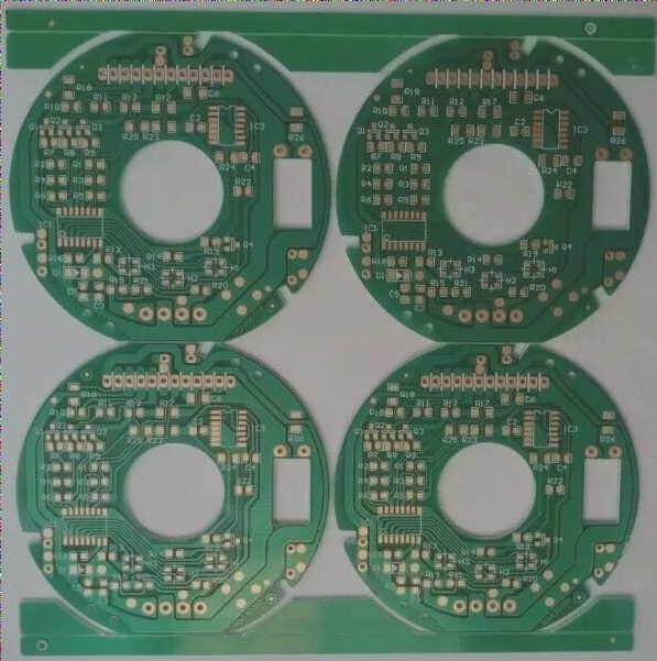
### Introduction to PCB Etching and Plating Methods
In printed circuit board (PCB) manufacturing, the process of defining the circuit pattern on the outer layer is critical. One common method is to apply a lead-tin anti-corrosion layer onto the copper foil in areas that will remain part of the circuit pattern. Subsequently, the remaining copper foil is chemically etched away, leaving behind the desired conductive paths. This process is known as **etching**.
**Etching vs. Engraving**
Etching and engraving are two primary techniques used to remove the excess copper foil from a PCB. Etching uses a chemical solution to dissolve the unwanted copper, while engraving is a physical process where a machine mechanically removes the copper. Etching, a chemical method, is more commonly used in PCB manufacturing because it allows for finer, more precise pattern definitions, while engraving is typically used for certain specialized applications.
### The Etching Process in PCB Manufacturing
The transformation of a raw PCB into a fully functional circuit board involves a combination of physical and chemical reactions. The most widely used method in PCB production is the **”pattern plating method.”** In this approach, a thin lead-tin layer is first plated on the copper foil areas that form the circuit pattern. The copper foil not covered by this protective layer is then subjected to an etching solution, which removes it, leaving behind the circuit traces.
**Etching and Engraving Methods:**
– **Chemical Etching**: This is the more commonly used method, involving the application of an etching solution that dissolves unwanted copper foil.
– **Engraving**: This is a mechanical method, using an engraving machine to physically remove copper. While less common, it can be used for certain high-precision applications.
### Challenges in PCB Etching: Undercut and Edge Control
One of the most common challenges in the etching process is the occurrence of **undercutting** and the formation of sharp edges. Undercutting refers to the undesirable lateral etching of the copper foil, which can compromise the accuracy and precision of the circuit pattern. The longer the PCB remains in the etching solution, the more pronounced the undercut becomes. Severe undercutting can lead to difficulties in producing fine lines and, in extreme cases, may render it impossible to fabricate certain circuit features.
**Undercutting and Edge Control**
To improve etching performance, it’s essential to reduce both undercutting and sharp edges. By doing so, the **etching coefficient** increases. A higher etching coefficient means better precision, allowing the etched traces to more closely match the original design. This is crucial for maintaining the integrity of thin wires and ensuring the accuracy of the final PCB.
In some cases, an excessively high plating resist (such as a tin-lead alloy, tin-nickel alloy, or nickel) can lead to short circuits. This happens because the protruding edges of the plated copper are more prone to breakage, potentially creating electrical bridges between two parts of the circuit. This issue underscores the importance of carefully managing plating thickness and etching parameters.
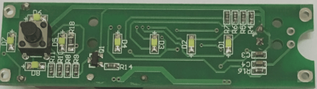
### Universal PCB Boards: Flexible, Cost-Effective, and Accessible
**Universal PCBs**, also known as **”hole boards”**, are versatile circuit boards pre-drilled with standard hole pitches (commonly 2.54mm). These boards allow users to easily insert components and create custom connections, making them ideal for prototyping and low-volume applications. Compared to professional PCB manufacturing, universal boards offer several advantages:
– **Low cost**: These boards are inexpensive and readily available.
– **Ease of use**: They require minimal expertise and are easy to handle.
– **Flexibility**: Users can create custom connections and designs based on their specific needs.
Universal PCBs are particularly useful in environments where speed is crucial, such as in **electronic design competitions**. In these competitions, where prototypes must be built quickly, universal PCBs are often used for their convenience and flexibility.
### Conclusion
The etching process is central to PCB manufacturing, enabling the precise definition of circuit patterns. Both chemical and mechanical methods, such as etching and engraving, play vital roles, with chemical etching being the most common due to its ability to achieve fine resolutions. However, challenges such as undercutting and sharp edges need to be carefully managed to ensure high-quality PCBs. Universal PCBs offer an affordable and flexible alternative, especially for prototyping and quick-turnaround projects.
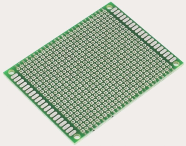
### Introduction to Universal PCB Boards
A **Universal PCB board** is a versatile printed circuit board designed for experimental use during the development and testing of electronic products. During the design phase, especially when quick iterations are needed, it is often impractical to rely on manufacturers to produce custom PCBs. In such cases, universal boards provide a convenient solution. These boards are pre-drilled with pads following a standard pitch (typically 2.54mm) and allow for flexible, quick connections during the experimental phase. Commonly known as “hole boards,” they offer a cost-effective, adaptable alternative to professional PCB fabrication, which is especially useful in scenarios such as student electronics competitions where designs must be completed rapidly.
### Key Considerations for Soldering on Universal PCB Boards
Proper soldering and component layout are essential to ensuring a functional and reliable circuit on a universal PCB board. Here are some important precautions to consider during the assembly process:
#### 1. **Component Layout and Planning**
The layout of components on a universal PCB board must be well thought out to optimize space and ensure signal integrity. Start by sketching the layout on paper or using simulation software before committing to soldering. For circuits that handle larger currents, pay attention to factors like contact resistance, ground loops, and wire capacitance. To mitigate ground loop interference, consider using single-point grounding techniques, which are often overlooked but critical for reliable performance.
#### 2. **Color-Coding Wires**
To avoid confusion during assembly and debugging, use different colored wires to represent different signals. Ideally, use the same color for all connections carrying the same signal to maintain clarity. This practice can make troubleshooting easier and speed up the process of identifying potential issues.
#### 3. **Step-by-Step Testing and Debugging**
It is important not to wait until the entire circuit is assembled before starting the testing and debugging process. Instead, test and debug individual sections of the circuit as you go. This approach allows you to isolate issues more efficiently and makes it easier to spot problems early before they propagate throughout the rest of the design.
#### 4. **Organized Wiring and Marking**
Ensure that your wiring follows a neat and organized pattern. This not only improves the overall look of the board but also makes debugging easier in the event of an issue. While soldering, always mark the corresponding pins on the schematic to ensure that each connection is made correctly.
#### 5. **Proper Soldering Techniques**
Pay attention to the soldering process, especially when tinning component leads. A clean and proper solder joint is essential for reliable electrical connections.
### Additional Soldering Tips
1. **Preparation of Pads**
If the pads on the universal board have become oxidized, gently polish them with fine sandpaper or a water-based abrasive cloth until they shine. Afterward, clean the pads with alcohol and apply a rosin solution before letting them dry. This helps ensure a solid connection when soldering.
2. **Cleaning Oxidized Component Leads**
If the component leads are oxidized, use a sharp blade or tool to carefully remove the oxide layer before proceeding with tinning. This step helps ensure proper solder adhesion.
3. **Wire Stripping**
When stripping insulation from wires, ensure that the stripping length is controlled to prevent the exposed wire from accidentally shorting against other components or wires.
4. **Tinning Wires**
Both ends of any wires that will be soldered should be tinned beforehand. This will make the soldering process smoother and ensure a solid connection.
5. **Following a Standard Soldering Process**
Stick to a standard, step-by-step soldering process to ensure that each joint is properly made. Following a reliable procedure reduces the risk of mistakes and improves the overall quality of the finished circuit.
### Etching Process and Quality Control
In addition to the soldering process, proper etching is crucial for creating clean and precise PCB traces. A few key considerations when etching include:
– **Undercutting and Edge Erosion:** To improve the accuracy of PCB traces, it’s important to minimize undercutting and edge erosion during the etching process. The longer the PCB stays in the etching solution, the more likely lateral etching (side erosion) will occur, which can result in jagged edges. Undercutting severely impacts trace accuracy and can prevent the creation of fine wires.
– **Increasing Etching Coefficients:** By reducing undercutting and edge erosion, you can increase the etching coefficient. A higher etching coefficient indicates the ability to maintain finer traces that closely match the original image, ensuring the precision of the design.
– **Managing Electroplating Quality:** Whether you are using a tin-lead alloy, tin, tin-nickel alloy, or nickel, be cautious with electroplating. Excessive plating can lead to issues such as short circuits, especially if the wire edges become too prominent and break easily. This can create electrical bridges between wires, causing malfunction in the circuit.
### Conclusion
Universal PCB boards offer a flexible and cost-effective solution for quick prototyping and experimentation in electronic design. By following best practices for layout, soldering, and etching, you can ensure that your circuit functions reliably and efficiently. These boards are an invaluable tool in educational settings, hobbyist projects, and rapid prototyping, where time and cost are critical factors. Proper planning, systematic testing, and attention to detail will make a significant difference in the quality and success of your projects.