Three Manufacturing Methods of Printed Circuit Boards (PCBs): Subtractive, MSAP, SAP
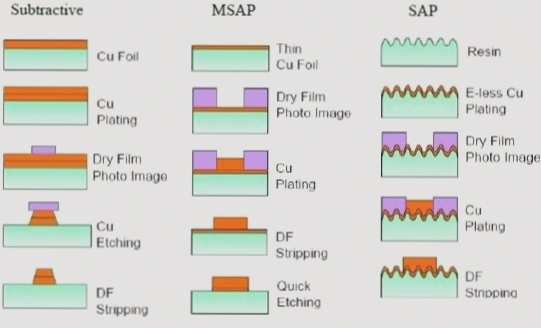
(1) **Subtractive Process**: The PCB laminate is initially covered with a layer of copper foil. A coating is applied to the lines that need to be retained, and the exposed copper foil is removed through etching to form the required circuit patterns.
(2) **MSAP (Modified Semi-Additive Process)**: A very thin layer of copper is first applied to the surface of the PCB material. Then, a coating is used to cover areas where copper is not needed, leaving the desired lines exposed. These exposed lines are then built up through electroplating. After removing the coating, the unthickened thin copper layer is removed by micro-etching, resulting in the final circuit pattern.
(3) **SAP (Semi-Additive Process)**: A preliminary copper circuit is formed directly on the plate using photocopying, printing, or laser activation. This circuit is then thickened through electroplating or electroless plating to achieve the final circuit pattern.

Three PCB Manufacturing Methods
With the emergence of new mSAP (Modified Semi-additive Process) technology in PCB manufacturing, trace widths can be reduced to as small as 1.25 mils, significantly increasing circuit assembly density. Currently, the advancement of integrated circuits has shifted focus from semiconductor IC lithography to PCB processes.
The most commonly used subtractive PCB process in the industry allows for a wiring width tolerance of up to 0.5 mils. Test results from WellCircuits indicate that for wiring widths exceeding 3 mils with relatively low signal edge rates, a 0.5 mil variation may not be obvious but can significantly impact impedance control for thinner wiring.
In PCB manufacturing, a copper-containing substrate material, known as Core, is used to cover one or both sides of the board. The material and thickness of copper substrates vary among PCB manufacturers, affecting insulation and mechanical properties.
The copper foil and substrate material are pressed together to form a substrate. This substrate is then coated with an anti-corrosion agent, exposed, and subjected to an acid bath that etches away the unexposed anti-corrosion agent and copper to form wiring. The goal is to create a rectangular cross-section for the wiring. However, during the acid bath process, copper on the vertical plane and part of the horizontal wiring wall can be eroded.
With strict control in the subtractive PCB process, wiring can achieve a trapezoidal cross-section of approximately 25 to 45 degrees. Improper control can lead to over-etching of the upper part of the wiring, resulting in a narrower top and thicker bottom. The etch factor, determined by comparing the height of the etched wiring to the eroded depth of the upper half, reflects how rectangular the cross-section of the wiring is.

1. Once routing can be done with rectangular traces, impedance becomes more predictable, and a repeatable layout can be achieved at nearly vertical angles. This means that circuit assembly density can be maximized, and PCB manufacturing yield can be improved from a signal integrity perspective.
2. One method to achieve this result is mSAP (Modified Semi-additive Process). In this approach, the substrate is laminated with a thin copper foil, typically 2 or 3 micrometers (μm) thick. Then, via holes are drilled and coated with electroless copper.
3. Next, an anti-corrosion agent is applied to specific areas for exposure to form the desired wiring. After the exposed areas are developed, the remaining copper is etched away. This method is essentially the opposite of the subtractive method. Unlike the subtractive method, which relies on chemical etching, mSAP utilizes photolithography for part of the wiring process. As a result, the width of the wiring formed using mSAP closely matches the original design specifications.
4. Under extremely tight tolerances, trace widths can be maintained at 1.25 mils with a certain level of impedance control. Measurements have shown that the impedance variation across the entire PCB board will not exceed 0.5 ohms, which is 1/5 of that observed with the subtractive method.
5. Test results from WellCircuits indicate that precise impedance control is essential to meet the demands of high-speed digital systems and microwave applications. This can be effectively achieved using mSAP. Furthermore, mSAP supports nearly vertical wiring designs and maximizes circuit assembly density.
(1) **Subtractive Process**: The PCB laminate is initially covered with a layer of copper foil. A coating is applied to the lines that need to be retained, and the exposed copper foil is removed through etching to form the required circuit patterns.
(2) **MSAP (Modified Semi-Additive Process)**: A very thin layer of copper is first applied to the surface of the PCB material. Then, a coating is used to cover areas where copper is not needed, leaving the desired lines exposed. These exposed lines are then built up through electroplating. After removing the coating, the unthickened thin copper layer is removed by micro-etching, resulting in the final circuit pattern.
(3) **SAP (Semi-Additive Process)**: A preliminary copper circuit is formed directly on the plate using photocopying, printing, or laser activation. This circuit is then thickened through electroplating or electroless plating to achieve the final circuit pattern.

Three PCB Manufacturing Methods
With the emergence of new mSAP (Modified Semi-additive Process) technology in PCB manufacturing, trace widths can be reduced to as small as 1.25 mils, significantly increasing circuit assembly density. Currently, the advancement of integrated circuits has shifted focus from semiconductor IC lithography to PCB processes.
The most commonly used subtractive PCB process in the industry allows for a wiring width tolerance of up to 0.5 mils. Test results from WellCircuits indicate that for wiring widths exceeding 3 mils with relatively low signal edge rates, a 0.5 mil variation may not be obvious but can significantly impact impedance control for thinner wiring.
In PCB manufacturing, a copper-containing substrate material, known as Core, is used to cover one or both sides of the board. The material and thickness of copper substrates vary among PCB manufacturers, affecting insulation and mechanical properties.
The copper foil and substrate material are pressed together to form a substrate. This substrate is then coated with an anti-corrosion agent, exposed, and subjected to an acid bath that etches away the unexposed anti-corrosion agent and copper to form wiring. The goal is to create a rectangular cross-section for the wiring. However, during the acid bath process, copper on the vertical plane and part of the horizontal wiring wall can be eroded.
With strict control in the subtractive PCB process, wiring can achieve a trapezoidal cross-section of approximately 25 to 45 degrees. Improper control can lead to over-etching of the upper part of the wiring, resulting in a narrower top and thicker bottom. The etch factor, determined by comparing the height of the etched wiring to the eroded depth of the upper half, reflects how rectangular the cross-section of the wiring is.

1. Once routing can be done with rectangular traces, impedance becomes more predictable, and a repeatable layout can be achieved at nearly vertical angles. This means that circuit assembly density can be maximized, and PCB manufacturing yield can be improved from a signal integrity perspective.
2. One method to achieve this result is mSAP (Modified Semi-additive Process). In this approach, the substrate is laminated with a thin copper foil, typically 2 or 3 micrometers (μm) thick. Then, via holes are drilled and coated with electroless copper.
3. Next, an anti-corrosion agent is applied to specific areas for exposure to form the desired wiring. After the exposed areas are developed, the remaining copper is etched away. This method is essentially the opposite of the subtractive method. Unlike the subtractive method, which relies on chemical etching, mSAP utilizes photolithography for part of the wiring process. As a result, the width of the wiring formed using mSAP closely matches the original design specifications.
4. Under extremely tight tolerances, trace widths can be maintained at 1.25 mils with a certain level of impedance control. Measurements have shown that the impedance variation across the entire PCB board will not exceed 0.5 ohms, which is 1/5 of that observed with the subtractive method.
5. Test results from WellCircuits indicate that precise impedance control is essential to meet the demands of high-speed digital systems and microwave applications. This can be effectively achieved using mSAP. Furthermore, mSAP supports nearly vertical wiring designs and maximizes circuit assembly density.


