What is the Gold Finger?
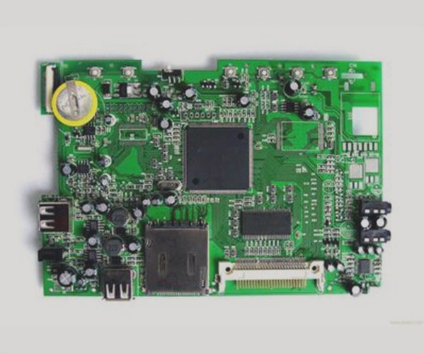
The gold finger is the connector located at the edge of a printed circuit board (PCB). Its shape resembles a finger, hence the name. It serves to protect the PCB prototypes from wear and tear. Below is an example image of a gold finger:

Surface Treatment of Gold Finger PCBs
Electroplated Nickel Gold: The thickness ranges from 3-50 microns. Due to its excellent conductivity, oxidation resistance, and wear resistance, it is commonly used in gold finger PCBs that require frequent insertion or mechanical friction. Despite the high cost of gold plating, it is only applied to specific areas such as the gold finger.
Immersion Gold: The conventional thickness is 1 micron, with a maximum of 3 microns. Immersion gold is widely used in high-precision PCBs with button positions, bonded ICs, BGAs, etc., due to its superior conductivity, flatness, and solderability. PCBs with lower wear resistance requirements can opt for full-board immersion gold. The cost of the immersion gold process is significantly lower than electroplating. The resulting finish is golden yellow.
Design Considerations for Gold Finger
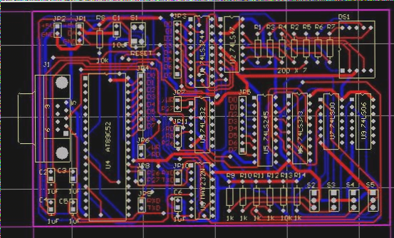
When designing a PCB with a shape and package similar to the example below, it is likely that the board has a gold finger. A quick method for identifying a gold finger is by checking if both the TOP and BOTTOM sides of the device have pins and a U-shaped groove, as shown below:

Here are some important design considerations for gold finger processing:
- For PCBs that require frequent insertion and removal, gold fingers should be plated with hard gold to enhance wear resistance.
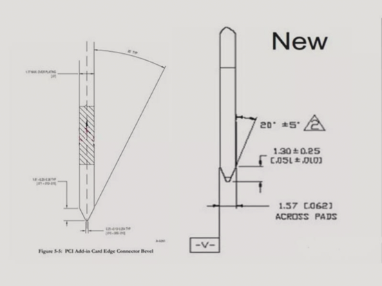
- The gold finger should be chamfered, typically at a 45° angle, although 20° or 30° angles can also be used. If no chamfer is specified in the design, it may cause issues. Below is an example showing a 45° chamfer:
- A solder mask window treatment should be applied to the gold finger area, while the PIN area does not require steel mesh openings.
- For immersion tin and immersion silver pads, a minimum distance of 14 mils from the tip of the gold finger is required. It is recommended that the pad be at least 1 mm away from the gold finger, including any via pads.
- Avoid placing copper on the surface of the gold finger.

Below is an example of a well-designed gold finger for reference:

- All inner layers beneath the gold finger should have copper cutting, typically with a width of 3 mm. In some designs, partial or full copper cutting is applied. For PCIe designs, the copper under the gold finger must be completely cut.
- Copper cutting beneath the gold finger helps reduce impedance differences between the gold finger and the signal line, which also aids in ESD protection.
- Recommendation: Full copper cutting beneath the gold finger pad.
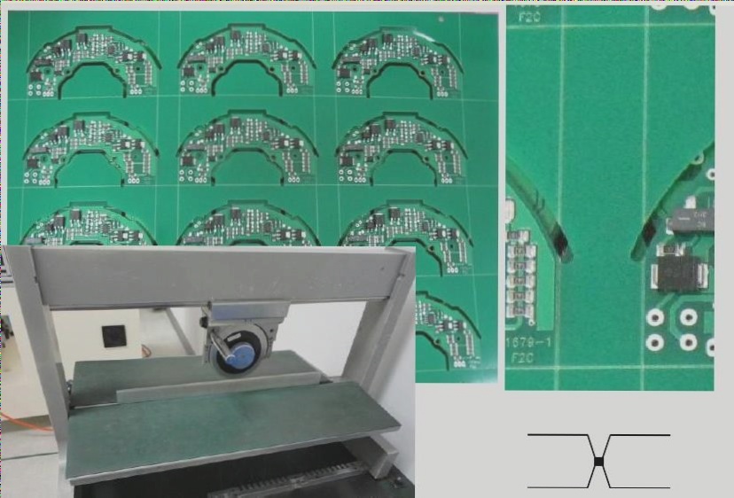
Processing and Production Considerations for PCB Gold Fingers
- PCBs with thicknesses between 1.2 mm and 2.4 mm can be processed with a beveled edge. Boards outside of this thickness range cannot be processed in this manner.
- The typical angle of the bevel is between 20° and 45°. Ensure there is adequate space between the gold finger and the edge of the board. Depending on the design or thickness of the PCB, the recommended distance between the gold finger and the board edge is 0.6 mm to 1.5 mm to prevent damage to the gold finger.
Below are several common diagrams illustrating different bevel angles and depths for your reference:


If you have any questions about PCBs or PCBA, feel free to reach out to me at
info@wellcircuits.com.