PCB Design Trends and Challenges
1. The demand for PCB design is increasing as data rates rise, pushing signal frequencies beyond 1 GHz. This technology involves RF and low-frequency microwave technologies, impacting system performance.
RF Engineering Challenges
2. RF engineering must combat electromagnetic field effects at higher frequencies, leading to unwanted crosstalk and return loss. Impedance mismatches can degrade signal quality by increasing noise and interference.

3. High return loss impacts signal quality by increasing system noise, making it harder for receivers to distinguish noise from the signal. To maintain signal integrity, it is recommended to keep total return loss at the highest frequency around -25dB, corresponding to a VSWR of 1.1.
Design Optimization
4. PCB design aims for smaller, faster, and cost-effective solutions. Managing ground planes, optimizing trace spacing, and impedance matching are crucial in addressing crosstalk and return loss issues.
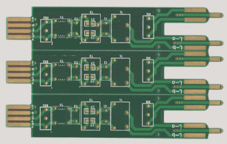
Interconnection Challenges
5. Interconnection points are critical in RF design, requiring thorough checks and addressing any issues. Chip-to-PCB interconnections, PCB-to-PCB connections, and signal input/output between PCBs and external devices are key considerations.
Chip-to-PCB Interconnection
6. High-speed chips like Pentium IV with numerous I/O points can process data at rates up to 1 GHz. Challenges lie in the high interconnection density, limiting further density increases. Innovative solutions, such as local wireless transmitters within chips, are emerging to address this issue.
7. IC design technology currently outpaces PCB design technology in high-frequency applications, highlighting the need for advancements in PCB technology.