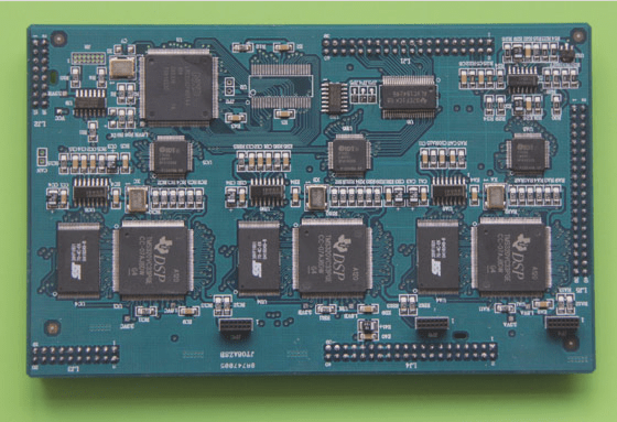
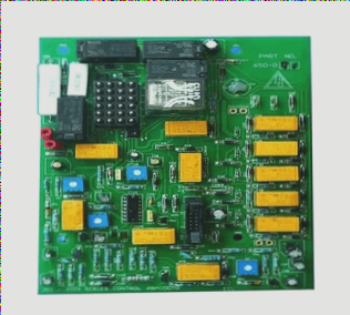
From the perspective of signal traces, a good PCB layering strategy involves placing all signal traces on one or several layers that are located next to the power layer or ground layer. For the power supply, a good layering strategy entails placing the power layer adjacent to the ground layer, with the smallest possible distance between them. This approach is known as the “layering” strategy.
A proper PCB layering strategy should include the following considerations:
1. Ensure that the wiring layer’s projection plane falls within its reflow plane layer area. If the PCB wiring layer extends beyond the reflow plane layer’s projection area, it may lead to signal lines being outside the projection area during wiring, resulting in “edge radiation” issues and an enlarged signal loop area, leading to increased differential mode radiation.
2. Strive to avoid placing adjacent wiring layers. Parallel signal traces on adjacent wiring layers can cause signal crosstalk. If it is unavoidable for wiring layers to be adjacent, increase the layer spacing between the two wiring layers appropriately, while reducing the layer spacing between the wiring layer and its signal loop.
3. Prevent overlapping of projection planes of adjacent plane layers. When the projections overlap, coupling capacitance between the layers can lead to noise coupling between the layers.
As an experienced FPC soft board manufacturer, WellCircuits Limited is proud to have collaborated with many clients. We are always ready to assist our new customers in any way possible. Please do not hesitate to reach out to us if you have any queries.