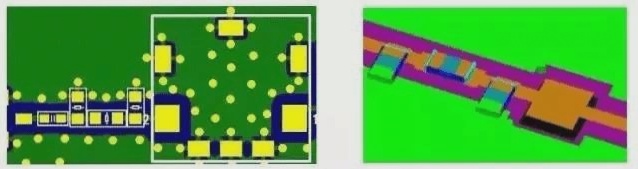
PCB Layer Configuration and Power Ground Separation Guidelines
When designing a PCB, it is crucial to carefully plan the layer configuration and consider the requirements for splitting power and ground planes. By following the best practices for PCB layer setting and power ground splitting, you can ensure optimal performance and reliability of your circuit board.
Key Considerations for PCB Layer Setting:
- Identify the signal integrity requirements of your design.
- Consider the frequency of operation and potential interference sources.
- Plan the layer stack-up to minimize crosstalk and signal distortion.
- Ensure proper impedance control for high-speed signals.
Guidelines for Power Ground Splitting:
- Separate the power and ground planes to minimize noise coupling.
- Use dedicated power planes for different voltage levels.
- Implement multiple ground planes for signal return paths.
- Place decoupling capacitors strategically to provide clean power to components.
By following these PCB layer setting and power ground splitting guidelines, you can optimize the performance of your PCB design and ensure the reliable operation of your electronic devices.