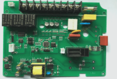
Effective Techniques to Improve PCB Design Deployment Rates
In PCB design, a variety of methods can be employed to enhance deployment rates and efficiency. By implementing the following techniques, project development cycles can be shortened for customers while ensuring high product quality:
1. Determining PCB Layer Count
Deciding on the size and layer count of the printed circuit board during the initial design stages is crucial. Factors such as the use of high-density ball grid array (BGA) components should be considered when determining the number of layers. The stack-up method and board size directly impact routing and trace impedance, influencing the overall design outcome. Opting for more layers initially and distributing copper evenly can help minimize last-minute wiring challenges and ensure compliance with design rules.
2. PCB Board Design Rules and Restrictions
Automatic routing tools require defined rules and constraints to efficiently accomplish wiring tasks. Different signal lines have varying requirements, necessitating categorization based on design criteria. Assigning priorities to signal classes ensures that stricter rules are applied where needed, covering aspects such as line width, via count, and layer restrictions. Adhering to these guidelines is essential for successful routing tool performance.
3. Layout of PCB Board Components
Design for Manufacturability (DFM) rules impose layout restrictions on components to streamline assembly processes. Optimizing circuitry and considering routing channels, via placements, and signal line layers during layout design are crucial for successful PCB assembly. Setting routing constraints and specifying signal line layers help routing tools achieve the desired design outcome.
4. PCB Board Fan-Out Design
Efficient fan-out design requires careful consideration of via placements to ensure proper connections between component pins. Utilizing optimal via sizes and line widths, along with considering online testing integration early in the design process, can enhance automatic wiring efficiency. Power and ground considerations play a significant role in fan-out and wiring design, impacting routing path options and inductive reactance.
5. Manual Wiring of PCB Board and Processing of Key Signals
While automatic routing tools are essential, manual routing remains crucial for handling critical signals effectively. Meticulous circuit design and post-routing signal path scrutiny are necessary for optimal performance. Manual routing of key signals allows for thorough inspection and correction before automating the remaining signals.
6. PCB Board Automatic Wiring
PCB Board Wiring Best Practices
- When wiring critical signals on a PCB, it is essential to control electrical parameters such as reducing distributed inductance and managing EMC to ensure optimal performance.
- EDA vendors offer tools that help in managing these parameters effectively, allowing for precise control over the routing process.
- Effective automatic routing follows specific guidelines, including limiting the use of layers and vias unless explicitly required, to optimize the layout.
- Excessive routing can lead to unnecessary layer and via usage, emphasizing the importance of adhering to routing constraints.
- After setting constraints, it is crucial to review the results to ensure they meet expectations, making adjustments as needed to accommodate signal and network wiring.
- Securing certain design areas is vital to prevent interference during subsequent manufacturing processes, enhancing the overall reliability of the PCB.
- Sequential routing of remaining signals should be approached with similar meticulousness, considering circuit complexity and predefined routing guidelines.
Design Considerations for Automatic PCB Wiring
- Adjust settings to simulate different routing scenarios and evaluate their impact on signal integrity and performance.
- Adhere to core routing principles while exploring variations in layers, line widths, and via types, such as blind holes and buried holes, to assess their effects on the design.
- Allow the routing tool to handle default networks when appropriate, leveraging automation for less critical signal paths.
Optimizing PCB Wiring Arrangement
Utilize EDA tools to analyze signal wiring lengths, identifying areas where vias and overall length can be reduced through manual adjustments. This phase helps distinguish between efficient and overly complex routing paths. Similar to manual designs, automatic routing should undergo thorough scrutiny and refinement during the inspection process.