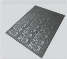
Pay attention to the following 10 aspects when designing PCB board layouts:

1. **PCB Routing Direction**: From the soldering surface’s perspective, the component arrangement should closely align with the schematic diagram. Ideally, the routing direction should match that of the circuit diagram. This alignment is essential because various parameters are tested on the soldering surface during production. Ensuring consistency with the circuit diagram facilitates inspection, debugging, and maintenance during the production process (Note: This assumes that circuit performance and the overall installation and panel layout requirements are met).

2. **Component Arrangement**: The placement of components on the PCB should be well-organized and evenly distributed, striving for neatness and aesthetic appeal while maintaining a strict structural layout.

3. **Resistor and Diode Placement**: There are two main placement orientations for resistors and diodes: horizontal and vertical.

(1) **Horizontal placement:** When the number of circuit components is small and the PCB size is large, horizontal placement is generally preferred. For resistors below 1/4W, when placed horizontally, the typical distance between the two pads is 4/10 inches. For a 1/2W resistor placed flat, the distance between the pads is typically 5/10 inches. For diodes, such as the 1N400X series rectifiers, the pad spacing is generally 3/10 inches; for the 1N540X series rectifiers, it is usually between 4 and 5/10 inches.

(2) **Vertical placement:** When there are numerous components and the PCB size is smaller, vertical placement is typically used. In this case, the pad spacing is generally between 1 and 2/10 inches.

**4. Potentiometer and IC holder placement principles**

(1) **Potentiometer:** Potentiometers are used in voltage regulators to adjust output voltage. In design, the potentiometer should be fully adjusted clockwise to increase the output voltage, and counterclockwise to reduce it. In adjustable constant current chargers, the central potentiometer adjusts the charging current. When designing the potentiometer, ensure that rotating it fully clockwise increases the current. The potentiometer should be placed in a location that meets the structural and layout requirements of the entire device, preferably on the edge of the board with the rotating knob facing outward.

(2) **IC holder:** When designing the PCB layout with IC holders, ensure that the positioning slot of the IC holder is correctly placed. Pay close attention to the pin orientation, ensuring that the first pin is located at either the lower right or upper left corner of the IC socket, adjacent to the positioning groove (viewed from the soldering side).

**5. Arrangement of input and output terminals**

(1) The distance between associated leads should not be too large, with 2 to 3/10 inches being an ideal range.

(2) Input and output terminals should be grouped together as much as possible, avoiding excessive dispersion.

**6. Pin arrangement sequence:** When designing the wiring diagram, ensure that the pin arrangement sequence is logical, and the component pin spacing is appropriate.

**7. Wiring design:** While meeting the performance requirements of the circuit, strive for efficient routing. Minimize the use of external jumpers and design the wiring to follow smooth, logical paths. The layout should be intuitive, easy to install, and facilitate repair and maintenance.

**8. PCB routing:** Minimize the number of bends in the PCB routing, ensuring that the traces are simple, clear, and direct.

**9. Trace width and pad spacing:** The width of the PCB traces and the line spacing should be reasonable. The distance between capacitor pads should ideally match the spacing of the capacitor’s lead pins.

**10. PCB design order:** The PCB design process should follow a logical sequence, such as from left to right and top to bottom, to ensure clarity and ease of assembly.

Leave a Comment

Contact

WellCircuits
More than PCB

Upload your GerberFile(7z,rar,zip)