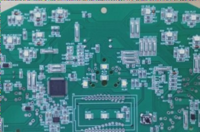
Light painting, often referred to as laser light plotter exposure, is a process in PCB manufacturing where the required patterns are transferred onto the film using precise light exposure. After the exposure, the film is washed, revealing the intended pattern. This same technique is used to transfer designs onto a PCB board. The pattern is transferred through a controlled exposure process, ensuring high precision and accuracy.
The typical workflow for producing a standard double-layer PCB involves several key steps:
1. **Material Cutting**: The base material is precisely cut to the required size for the PCB.
2. **Drilling**: Holes are drilled into the material to accommodate vias and other connections.
3. **Copper Thickening**: A copper layer is thickened to the desired specifications to ensure proper conductivity.
4. **Outer Layer Graphics**: The pattern for the outer layers is created, typically using the light exposure technique.
5. **External Image Inspection**: After pattern creation, external image inspection ensures that the graphics align correctly and meet design specifications.
6. **Solder Mask**: A solder mask layer is applied to prevent solder from bridging connections and to protect the copper circuitry.
7. **Solder Mask Inspection**: The solder mask is carefully inspected for defects or misalignments before moving on to the next step.
8. **Character Printing**: Necessary labeling and text, such as component designators, are printed onto the board.
9. **Surface Treatment**: The surface of the PCB is treated to improve solderability and prevent oxidation.
10. **Molding**: The PCB is molded into its final shape, often involving encapsulation or coating.
11. **Testing**: The PCB undergoes various tests to verify functionality and integrity, including electrical testing.
12. **Drawing Test Lines**: Test lines are drawn to check electrical paths and to ensure the PCB meets all design requirements.
13. **FQC (Final Quality Control)**: A final inspection is performed to ensure the board meets all specifications and quality standards.
14. **FQA (Final Quality Assurance)**: An additional round of quality checks is done before packaging.
15. **Packaging and Shipment**: The completed and inspected PCBs are packaged and prepared for shipment.
This structured process ensures that the final PCB meets both functional and quality requirements, with multiple checkpoints to identify and correct any issues. The overall focus is on precision, reliability, and performance, making sure the PCB is ready for use in various electronic applications.

**PCB Light Painting Process: File Verification, Technical Review, and Conversion Guidelines**
1. **File Verification and Integrity Check**
– **File Condition:** Begin by verifying the integrity of the provided PCB files. Ensure that they are complete and free from errors.
– **File Safety:** Check for any malicious content in the files. If the files are infected, they must undergo disinfection before proceeding.
– **Gerber File Check:** For Gerber files, confirm whether a D-code table is included or if the D-codes are embedded in the files. This is crucial for defining the specific manufacturing details like pad shapes, hole sizes, and trace widths.
2. **Technical Level Review Against Factory Capabilities**
– **Spacing Requirements:** Inspect the various spacing values in the customer’s PCB design files, including the line-to-line, line-to-pad, and pad-to-pad distances. These spacings should be larger than or equal to the minimum spacing the factory can process. The factory’s process capabilities determine the minimum spacing thresholds.
– **Trace Width:** Verify that the trace width in the design meets or exceeds the minimum trace width that the factory’s manufacturing process can support. This ensures reliable signal integrity and reduces the risk of manufacturing defects.
– **Via Hole Size:** Check the via hole diameters in the design to ensure they are above the minimum size that the factory’s process can handle. This is critical to ensure proper electrical connection and reliable signal transmission through the PCB.
– **Pad Size and Aperture:** Evaluate the pad dimensions and the internal apertures to ensure they meet factory capabilities. Pads should be large enough that after drilling, the pad edges maintain a sufficient width, ensuring a strong electrical connection and good mechanical stability.
3. **Determining Process Requirements for PCB Light Painting**
– **Mirrored Film Decision:** The light painting process may require a mirrored film, depending on the subsequent manufacturing processes. The choice of film mirroring is typically based on the process being used:
– **Negative Film Process:** For processes like screen printing or dry film, the copper side of the substrate will be the reference. This means that the film should have the copper surface facing outward.
– **Diazo Film Process:** In this process, the film is inherently mirrored during exposure. As a result, the copper side should be the inner (non-film) surface, with the copper side not exposed.
– **Unit Film Requirement:** If the PCB light painting involves using a single unit film instead of an imposition film, an additional mirroring step may be necessary.
– **Solder Mask Expansion Guidelines:**
– **Avoiding Wire Exposure:** The solder mask should be designed to avoid covering traces that run close to pads. If the solder mask is too small, the pad edges may be exposed due to slight deviations during manufacturing.
– **Pad Coverage:** The solder mask should be slightly larger than the pads to accommodate any operational deviations. However, the mask should not be excessively large, as this could lead to unintended exposure of the underlying traces.
– **Compensation for Deviations:** Considering that deviations can occur during the solder mask application process, it’s essential to ensure that the solder mask is expanded enough to compensate for these errors without compromising trace integrity.
4. **Conversion of CAD Files to Gerber Files**
– **Standardization for CAM Processing:** To streamline the production process, all CAD files should be converted into the standard Gerber format used by PCB light plotters. This also includes generating the equivalent D-code table.
– **Process-Specific Parameters:** When converting files, it is important to adhere to specific process parameters that may need to be adjusted during the conversion.
– **CAD Software Compatibility:** Most commonly used CAD software (except for PCB Work and Tango) can directly convert to Gerber format. If using PCB Work or Tango, the files should first be converted to Protel format using appropriate tool software before converting them to Gerber.
By following these structured guidelines, manufacturers can ensure that PCB designs are compatible with the factory’s process capabilities, avoid production errors, and achieve optimal outcomes for the final product.
The typical workflow for producing a standard double-layer PCB involves several key steps:
1. **Material Cutting**: The base material is precisely cut to the required size for the PCB.
2. **Drilling**: Holes are drilled into the material to accommodate vias and other connections.
3. **Copper Thickening**: A copper layer is thickened to the desired specifications to ensure proper conductivity.
4. **Outer Layer Graphics**: The pattern for the outer layers is created, typically using the light exposure technique.
5. **External Image Inspection**: After pattern creation, external image inspection ensures that the graphics align correctly and meet design specifications.
6. **Solder Mask**: A solder mask layer is applied to prevent solder from bridging connections and to protect the copper circuitry.
7. **Solder Mask Inspection**: The solder mask is carefully inspected for defects or misalignments before moving on to the next step.
8. **Character Printing**: Necessary labeling and text, such as component designators, are printed onto the board.
9. **Surface Treatment**: The surface of the PCB is treated to improve solderability and prevent oxidation.
10. **Molding**: The PCB is molded into its final shape, often involving encapsulation or coating.
11. **Testing**: The PCB undergoes various tests to verify functionality and integrity, including electrical testing.
12. **Drawing Test Lines**: Test lines are drawn to check electrical paths and to ensure the PCB meets all design requirements.
13. **FQC (Final Quality Control)**: A final inspection is performed to ensure the board meets all specifications and quality standards.
14. **FQA (Final Quality Assurance)**: An additional round of quality checks is done before packaging.
15. **Packaging and Shipment**: The completed and inspected PCBs are packaged and prepared for shipment.
This structured process ensures that the final PCB meets both functional and quality requirements, with multiple checkpoints to identify and correct any issues. The overall focus is on precision, reliability, and performance, making sure the PCB is ready for use in various electronic applications.
**PCB Light Painting Process: File Verification, Technical Review, and Conversion Guidelines**
1. **File Verification and Integrity Check**
– **File Condition:** Begin by verifying the integrity of the provided PCB files. Ensure that they are complete and free from errors.
– **File Safety:** Check for any malicious content in the files. If the files are infected, they must undergo disinfection before proceeding.
– **Gerber File Check:** For Gerber files, confirm whether a D-code table is included or if the D-codes are embedded in the files. This is crucial for defining the specific manufacturing details like pad shapes, hole sizes, and trace widths.
2. **Technical Level Review Against Factory Capabilities**
– **Spacing Requirements:** Inspect the various spacing values in the customer’s PCB design files, including the line-to-line, line-to-pad, and pad-to-pad distances. These spacings should be larger than or equal to the minimum spacing the factory can process. The factory’s process capabilities determine the minimum spacing thresholds.
– **Trace Width:** Verify that the trace width in the design meets or exceeds the minimum trace width that the factory’s manufacturing process can support. This ensures reliable signal integrity and reduces the risk of manufacturing defects.
– **Via Hole Size:** Check the via hole diameters in the design to ensure they are above the minimum size that the factory’s process can handle. This is critical to ensure proper electrical connection and reliable signal transmission through the PCB.
– **Pad Size and Aperture:** Evaluate the pad dimensions and the internal apertures to ensure they meet factory capabilities. Pads should be large enough that after drilling, the pad edges maintain a sufficient width, ensuring a strong electrical connection and good mechanical stability.
3. **Determining Process Requirements for PCB Light Painting**
– **Mirrored Film Decision:** The light painting process may require a mirrored film, depending on the subsequent manufacturing processes. The choice of film mirroring is typically based on the process being used:
– **Negative Film Process:** For processes like screen printing or dry film, the copper side of the substrate will be the reference. This means that the film should have the copper surface facing outward.
– **Diazo Film Process:** In this process, the film is inherently mirrored during exposure. As a result, the copper side should be the inner (non-film) surface, with the copper side not exposed.
– **Unit Film Requirement:** If the PCB light painting involves using a single unit film instead of an imposition film, an additional mirroring step may be necessary.
– **Solder Mask Expansion Guidelines:**
– **Avoiding Wire Exposure:** The solder mask should be designed to avoid covering traces that run close to pads. If the solder mask is too small, the pad edges may be exposed due to slight deviations during manufacturing.
– **Pad Coverage:** The solder mask should be slightly larger than the pads to accommodate any operational deviations. However, the mask should not be excessively large, as this could lead to unintended exposure of the underlying traces.
– **Compensation for Deviations:** Considering that deviations can occur during the solder mask application process, it’s essential to ensure that the solder mask is expanded enough to compensate for these errors without compromising trace integrity.
4. **Conversion of CAD Files to Gerber Files**
– **Standardization for CAM Processing:** To streamline the production process, all CAD files should be converted into the standard Gerber format used by PCB light plotters. This also includes generating the equivalent D-code table.
– **Process-Specific Parameters:** When converting files, it is important to adhere to specific process parameters that may need to be adjusted during the conversion.
– **CAD Software Compatibility:** Most commonly used CAD software (except for PCB Work and Tango) can directly convert to Gerber format. If using PCB Work or Tango, the files should first be converted to Protel format using appropriate tool software before converting them to Gerber.
By following these structured guidelines, manufacturers can ensure that PCB designs are compatible with the factory’s process capabilities, avoid production errors, and achieve optimal outcomes for the final product.