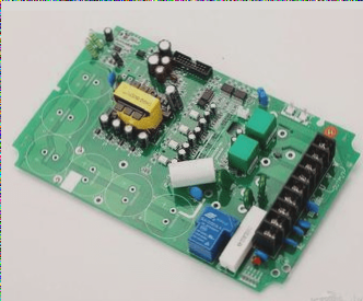
Important Design Parameters for PCB Layout
-
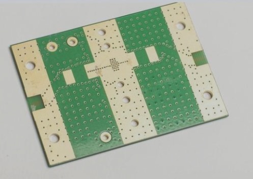
Vias (Conductive Holes)
- Minimum Aperture: 0.3mm (12mil)
- Minimum VIA Hole Diameter: 0.3mm (12mil)
- Via Hole to Hole Spacing: ≥6mil
- Pad to Outline Spacing: 0.508mm (20mil)
-
Line Design
- Minimum Line Spacing: 6mil (0.153mm)
- Minimum Line Width: 6mil (0.153mm)
- Line to Outline Line Spacing: 0.508mm (20mil)
-
PAD Pad (Plug-in Hole)
- Outer Ring of Plug-in Hole: ≥0.2mm (8mil)
- Plug-in Hole to Hole Spacing: ≥0.3mm
- Size of Plug-in Hole: Must be larger than component pins
- Pad to Outline Spacing: 0.508mm (20mil)
-
Solder Mask
- SMD Window Size: ≥0.1mm (4mil)
-
Character Design
The character width should be ≥0.153mm (6mil) and the height should be ≥0.811mm (32mil). The ideal ratio between width and height is 5.
-
Non-Metallized Slot Holes
Minimum Spacing of Slot Holes: ≥1.6mm
-
Imposition
- Imposition Gap for Gap Imposition: ≥1.6mm
- Gapless Imposition Gap: ~0.5mm
- Process Edge: ≥5mm
Latest Information: When designing PCB layouts, it is crucial to consider the size and spacing of vias, lines, pads, solder masks, characters, slot holes, and imposition to ensure smooth production and high-quality results. Keeping these design parameters in mind will help in creating efficient and reliable printed circuit boards.