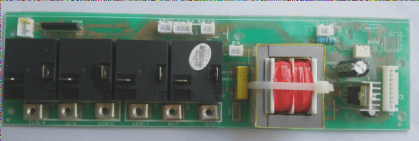
PCB Manufacturing Methods
-
Screen Printing Method
The PCB, or printed circuit board, is created using the screen printing technique. The process involves design layout, tracing, exposure, printing, etching, surface treatment, soldering, and finalizing the board. This method is ideal for mass production but is rarely used in laboratories.
-
Engraving Method
Utilizing a specialized engraving machine, this method removes excess copper foil to establish electrical connections. While offering high precision, it operates at a slower speed and higher cost.

-
Freehand Method
Using a pen to apply anti-corrosion paint directly onto copper-clad laminate, followed by chemical etching. Hand-drawing is challenging due to the compact nature of modern electronic components.
-
Layout Method
Electronics stores offer pre-cut symbols and tape for circuit design. Symbols and tape are adhered to the copper foil surface using a soft hammer for etching.
-
Pre-coated Photosensitive Copper Clad Laminate
This method involves using a photosensitive board with a pre-coated layer for PCB production. The process includes printing the design, exposing it to UV light, developing, and etching.
-
Thermal Transfer Method
Graphics are printed on thermal transfer paper with a laser printer, then transferred to the copper-clad board using heat. The toner forms a protective layer on the board, providing corrosion resistance.