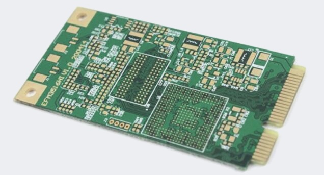
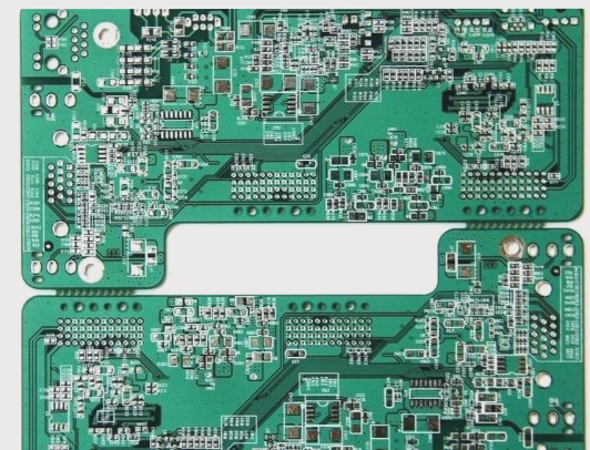
1. Nowadays, an increasing number of electronic products and communication industries utilize HDI PCB circuit boards.
2. So, what exactly is an HDI circuit board?
3. HDI (High-Density Interconnect) boards are high-density circuit boards that leverage micro-blind via technology.
4. This process incorporates both internal and external circuits, facilitating connections between the internal components of each layer through drilling and metallization of the holes.
5. Customized HDI boards typically feature microvias, buried vias, and blind vias.
6. Micro-holes: In printed circuit boards, holes with a diameter of less than 6 mm (150 microns) are referred to as micro-holes.
7. Buried holes: Buried vias are not visible in the finished product.
8. They are primarily used to conduct inner lines, which can help reduce signal interference and maintain the continuity of the transmission line’s characteristic impedance.
9. Since buried vias do not occupy the surface area of the PCB, more components can be placed on the board’s surface, thereby minimizing the overall footprint.
10. Blind vias: These are through holes that connect the surface layer to the inner layer without passing through the entire board.
—
Let me know if you need any more adjustments!

With the advancement of electronic products towards higher density and precision, similar demands have emerged for PCB circuit boards. The most effective method to enhance PCB density is to minimize the number of through holes, while accurately incorporating blind and buried vias to fulfill this requirement, thus facilitating the production of HDI boards. The HDI circuit board not only reduces the production footprint but also maintains relatively stable signal and electrical performance.
1. The issue of layer alignment in the production of blind and buried multi-layer printed circuit boards
Utilizing the pin front positioning system of conventional multi-layer printed board manufacturing, the graphic production for each layer and individual chip is standardized within a positioning framework, enabling successful manufacturing. For the ultra-thick single chip in this case, if the board thickness reaches 2 mm, it is possible to mill a specific layer thickness at the positioning hole location, thanks to the capabilities of the four-slot positioning hole punching equipment integrated into the front positioning system.
2. Glue flow on the board surface post-lamination
Given the characteristics of manufacturing blind and buried via multi-layer printed circuit boards, the chosen process inevitably leads to glue flow on both sides of the board after lamination. To ensure the accuracy of graphic transfer in subsequent processes and to meet electroplating adhesion requirements, manual removal of the glue from the board surface is necessary. This task poses challenges and inconveniences for operators. Therefore, during the lamination phase, we selected two materials for release isolation: one is the currently used polyester film, and the other is PTFE film. Comparative experiments indicate that the laminate using PTFE film as the release isolation material exhibits significantly better surface flow than that using polyester film. This finding also offers a reference for addressing similar issues in the future.
3. Position accuracy and alignment challenges in graphic transfer
As is well known in the industry, during the manufacturing of blind and buried multi-layer printed circuit boards, silver salt stencils are typically used for producing each inner layer pattern, in conjunction with consistent four-slot positioning holes for graphic transfer. Before transferring each inner layer graphic, each inner layer board undergoes numerical control drilling and hole metallization, which presents a protection challenge for the four-slot positioning holes. Moreover, after lamination is complete, various methods are commonly employed for transferring outer layer graphics:
A. Utilizing the diazo film template copied from the silver salt film template, with separate alignment on both sides;
B. Employing the original silver salt sheet template, positioning the board according to the four-slot positioning holes;
C. When creating the template, in addition to designing the four-slot positioning holes, incorporating two additional positioning holes outside the effective graphic area. This allows for positioning and manufacturing the outer layer pattern through these two additional holes.
Each of these three methods has its advantages and disadvantages. To ensure layer overlap, some face challenges regarding the protection of four-slot positioning holes at different manufacturing stages; others struggle with the concentricity of the two-sided graphics after milling; and some encounter issues with the asymmetry of the graphics centers on both sides, attributed to pressure factors and borehole offsets.


