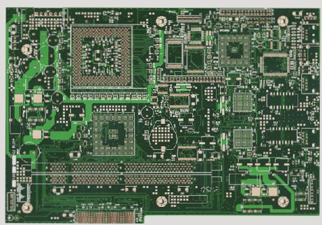
Reducing Interference Between Digital and Analog Signals on PCB Boards
Before designing a PCB board, it is essential to understand the principles of electromagnetic compatibility (EMC) to minimize interference between digital and analog signals. Two basic principles to consider:
- Minimize the current loop area.
- Utilize only one reference plane to prevent the formation of a dipole antenna.
Key Points to Address Interference:
- Separate digital ground and analog ground on a mixed-signal circuit board to achieve isolation, but be cautious of potential signal line crossings.
- EMI issues can arise from signal lines crossing ground or power supplies, especially in segmented grounds.
- Optimizing mixed-signal circuit board design involves understanding the current return path and minimizing loop area.
- Consider using optical isolation devices, transformers, or differential signals to reduce interference between segmented grounds.
- High-frequency current characteristics play a crucial role in assessing digital signal interference on analog signals.
- Unified partitioning of PCB into analog and digital regions is preferred to prevent digital ground currents from disrupting analog signals.
- Adherence to proper signal routing and thorough verification of wiring compliance are essential in effective PCB design.
Manufacturers recommend linking AGND and DGND pins of A/D converters to a low-impedance ground via short leads to prevent digital noise coupling to analog circuits within the IC.
Conclusion:
By following these guidelines and understanding the intricacies of signal routing, PCB designers can minimize interference between digital and analog signals, ensuring optimal performance of the circuit board.
Essential Considerations for Mixed-Signal PCB Design
When working with systems that incorporate multiple A/D converters, it is crucial to connect AGND and DGND under each converter carefully. This connection should match the IC width precisely to prevent signal line interference and maintain ground isolation, as illustrated in Figure 4.
It is important to follow manufacturer guidelines to avoid compromising ground isolation, especially when dealing with sensitive applications like medical devices, industrial equipment, or PCB layouts with strict design requirements.
Key Aspects of Mixed-Signal PCB Design
- Partitioning into analog and digital segments
- Optimal component placement
- Strategic positioning of A/D converters
- Minimizing ground division
- Separate routing of digital and analog signals
- Segregation of power sources
- Proper wiring practices
- Analysis of current flow
- Compliance with regulations and thorough testing
By following these guidelines and considering these aspects at each stage of the design process, you can ensure the effectiveness and reliability of your mixed-signal PCB layout.