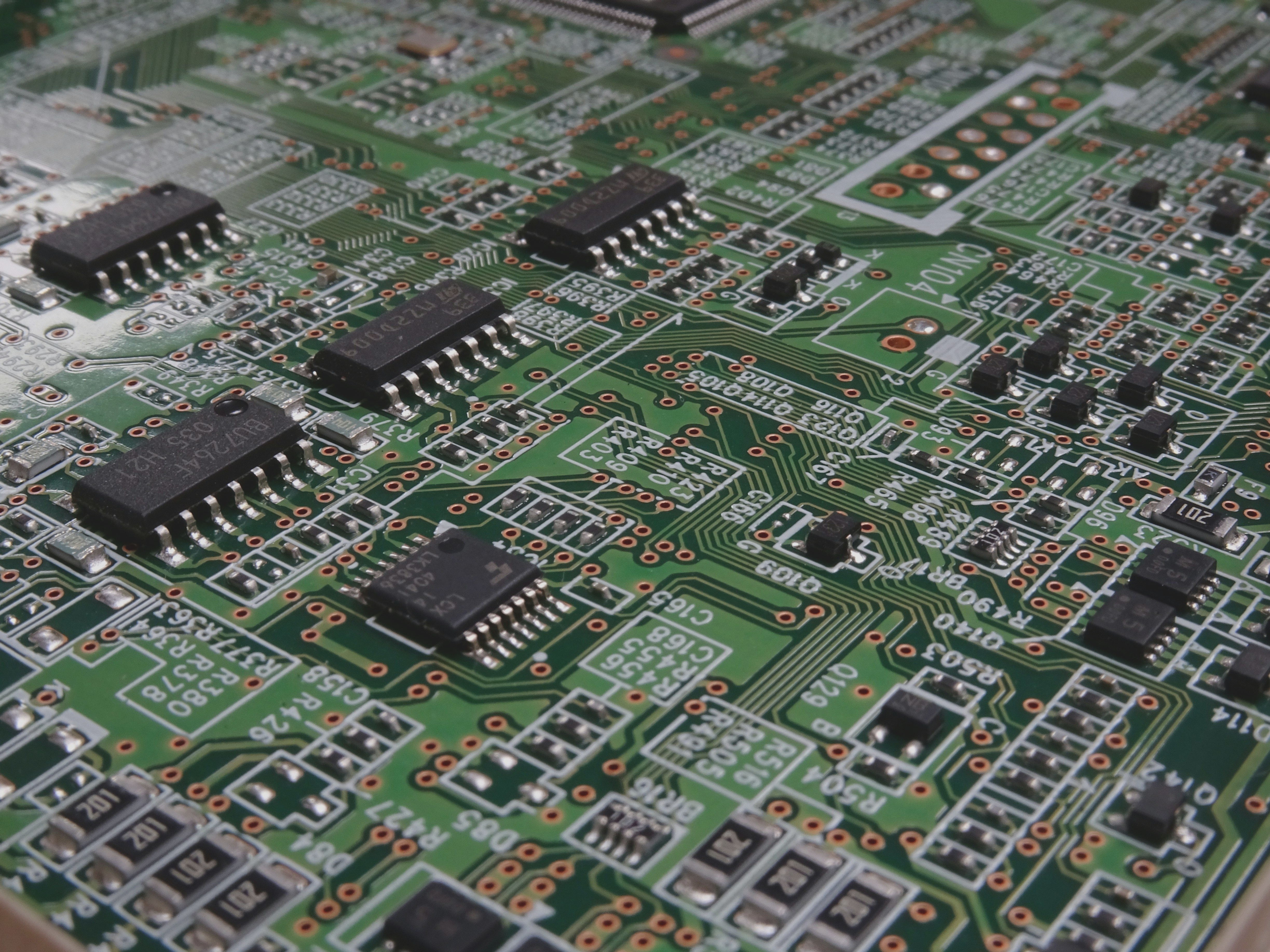
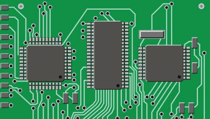
PCB Online Test Fixture Design Rules for Cost and Complexity Reduction
- The test fixture, also known as a bed of needles, is essential for the bare board test process.
- Flexible test needles on the fixture require a relatively large test pad area.
- Conducting one-sided testing of the assembled board can help reduce the cost of the test fixture during in-line testing.
Verified Design Rules to Reduce Test Fixture Cost and Complexity:
- Ensure the diameter of test pads is proportional to the hole size, with a minimum diameter of 0.9 mm.
- Maintain a clearance around the test probe based on the assembly process, with a minimum of 0.6 mm.
- Limit the height of components on the test surface of the probe to 5.7 mm.
- Avoid placing components or test pads within 3 mm from the edge of the circuit board.
- Apply flux or conductive non-oxidizing coating to all probe areas.
- Ensure the probe contact point is on the pad, not on the end point, especially on leadless SMT component arrays and pin components.
- Utilize probes to test both sides of the circuit board for increased reliability and cost-effectiveness.
- Use standard probes with the center hole of the test pad set at 2.5 mm if feasible.
- Minimize the use of gold fingers as test pads to avoid potential damage from test probes.
- Distribute test pads evenly across the circuit board to prevent bending, probe failure, and vacuum sealing issues.