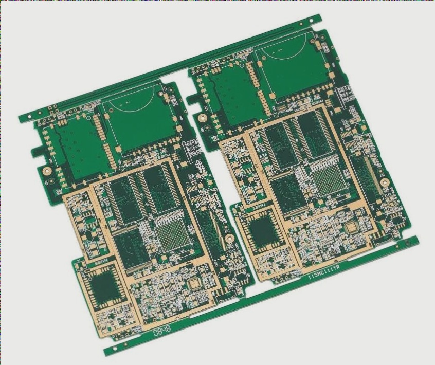
PCB Size Considerations
- The size of a PCB is crucial in electronic processing line equipment capacity.
- Standard PCB sheet sizes are typically 20″×24″ (508mm×610mm).
- Recommended PCB sizes match equipment in the production line for efficiency.
- Small PCBs can be designed in patches to enhance production efficiency.
Design Guidelines for PCB Size
- Maximum PCB size should generally be 460mm×610mm.
- Recommended size range is (200~250) mm×(250~350) mm with a 2:1 length-width ratio.
- For 125mm×125mm PCBs, appropriate sizing is essential.
PCB Shape and Transmission
- Regular square shape with rounded corners is ideal for PCBs.
- Irregular PCB shapes should be pieced into standard squares for stability.
- Beveled golden finger designs aid insertion during assembly.
Edge Requirements
- Process board edge size depends on equipment guide rail requirements.
- Transmission side width should be a minimum of 5.0mm without components or solder joints.
- Non-transmission edge should ideally have a 2.5mm component-free zone.
Positioning Holes and Symbols
- Each PCB should have at least two positioning holes for accuracy.
- Optical positioning symbols are essential for modern equipment.
- Global and local fiducials aid in precise positioning during production.
PCB Optical Positioning Symbol Design Guidelines
- The optical positioning symbol can be designed in various shapes such as square, diamond, round, cross, or well shape, with a height of 2.0mm.
- It is recommended to design a Ø 1.0 m round copper definition graphic for general use, ensuring color contrast with the environment. Leave a 1mm space around the optical position mark in the welding area, avoiding any characters. The copper foil presence under the three symbols on the same panel should be consistent.
- For PCBs with patch components, place three whole-board optical positioning symbols at the corners to aid in three-dimensional positioning and solder paste thickness detection.
- When dealing with Mosaic, include two or three optical positioning symbols on the diagonal of each unit board in addition to the whole-board symbols.
- For QFP devices with lead center distance ≤0.5mm and BGA devices with lead center distance ≤0.8mm, set local optical positioning symbols diagonally for precise positioning.
- In cases of mounting components on both sides, ensure optical positioning symbols are present on each side.
- When there are no positioning holes on the PCB, position the center of the optical symbol at least 6.5mm away from the PCB edge. If there are positioning holes, design the symbol near the center of the PCB on the side of the positioning hole.