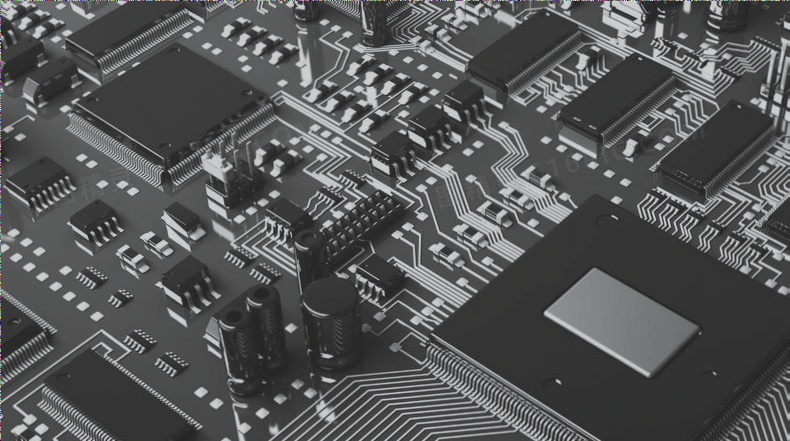
Mastering the Art of PCB Design
To become a top-notch PCB expert, one must adopt a comprehensive approach similar to that of a visionary. Understanding the full spectrum of a PCB project involves grasping every detail from its inception to the final stages, while also acknowledging crucial elements that require careful attention throughout the process. Let’s explore the detailed steps involved in a PCB project:
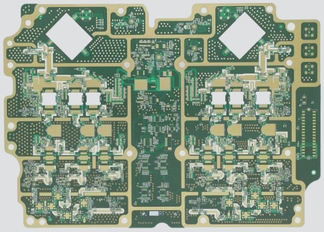
1. Scrutinizing the Structural Schematic
- Focus on dimensions of screw and positioning holes
- Identify areas for device and wiring exclusion
- Consider height constraints and connector placement
2. Layout Design Principles
Going beyond the physical structure, the core principle of layout design revolves around aligning signal and power flow paths.
3. Adhering to Design Rules
- Ensure proper line length and impedance
- Consider topological factors and stack structure
4. Critical Parameters for Examination
Key parameters like line impedance, reference surface continuity, EMC compliance, signal/power integrity, and adherence to Design for Manufacturability (DFM) standards require thorough examination and adherence.