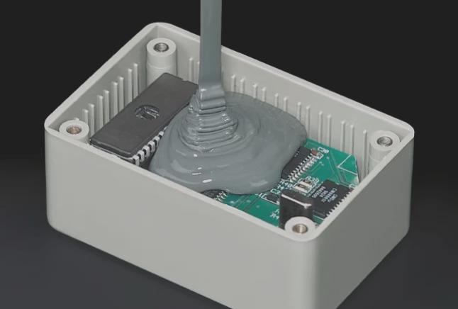
PCB potting is a process in which a printed circuit board (PCB) or an electronic component is coated or submerged in a protective material, typically a liquid or gel-like substance known as a potting compound. Depending on the application, three common materials are used: epoxy, polyurethane, and silicone.
During the potting process, the electronic assembly is carefully positioned inside a mold, often referred to as the “pot.” This mold serves as a temporary container and shaping tool throughout the potting procedure. The selected potting compound is then poured into the mold. Once cured or hardened, the compound permanently encapsulates and protects the electronic assembly, offering the required protective properties.

Figure 1: Example of PCB potting
Advantages of PCB Potting
The potting compound helps protect the components by preventing moisture and corrosive agents from reaching them. Additionally, it provides resistance to shock and vibration. For example, potting helps to avoid the formation of air pockets and bubbles within the electronic components. These imperfections can compromise the thermal conductivity, mechanical strength, and electrical insulation properties of the potting material. Moreover, air pockets can trap moisture and other contaminants, leading to further issues.
Applications of PCB Potting
PCB potting has a wide range of applications across multiple industries. In the automotive sector, it is used to protect sensitive electronics in vehicles from extreme temperatures, vibrations, and corrosive substances encountered on the road. In aerospace and marine applications, potting plays a vital role in ensuring the reliability and durability of electronics exposed to harsh environmental conditions.
How does potting compare to conformal coating?
As an alternative to potting, some PCBs or components are coated with a thin layer of transparent conformal coating. While both methods provide protective barriers, how do you decide between the two options?
Protection Strength: The thickness of the protective layer is a key factor in determining the strength of protection provided by both conformal coating and potting. Conformal coatings are typically applied in thicknesses ranging from 25 to 250 micrometers, using materials such as acrylics, silicones, urethanes, and epoxies. In contrast, potting materials are generally applied at a thickness of 1 to 10 millimeters. As a result, potting offers superior protection compared to conformal coating but adds more weight and volume to the device. For example, conformal coating is commonly used in mobile and handheld electronics, while potting is employed in more demanding environments where enhanced protection is necessary.
Flexibility and Rework:
When it comes to flexibility, conformal coating offers greater versatility and ease of modification than potting. Its thinner application allows for rework, repairs, or adjustments if needed, making it ideal for applications where future changes are anticipated. Various rework methods, such as solvent-based, mechanical, thermal, and chemical stripping, can be used. On the other hand, once the potting material has cured, it forms a rigid and immovable protective shell around the components, making it less flexible and more difficult to modify or rework after encapsulation.
In summary, potting is preferred when maximum protection is required, especially in harsh or extreme environments. On the other hand, conformal coating offers a balance between protection and flexibility, making it suitable for applications where adaptability, modifications, and considerations of weight and volume are important. Ultimately, the choice depends on the specific requirements and priorities of the application.
If you have any questions regarding PCBs or PCBA, please feel free to contact us at info@wellcircuits.com.


