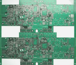
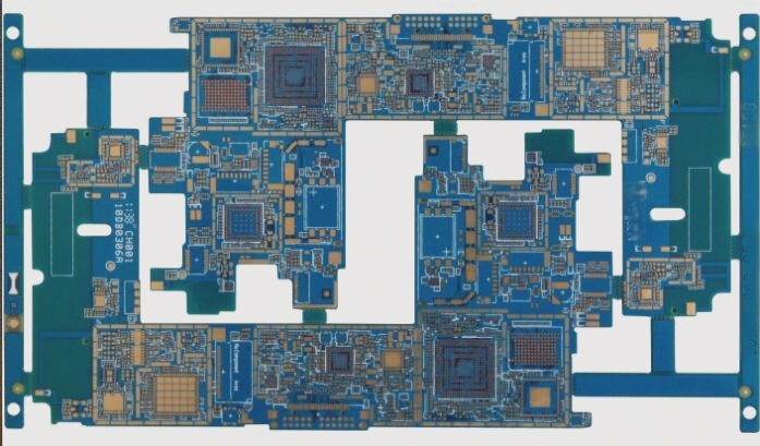
2: The substrate needed for PCBs, typically FR4, consists mainly of epoxy resin and fiberglass cloth.
3: The number of PCB layers significantly impacts pricing; however, the prototype PCB process remains consistent across different layer counts.
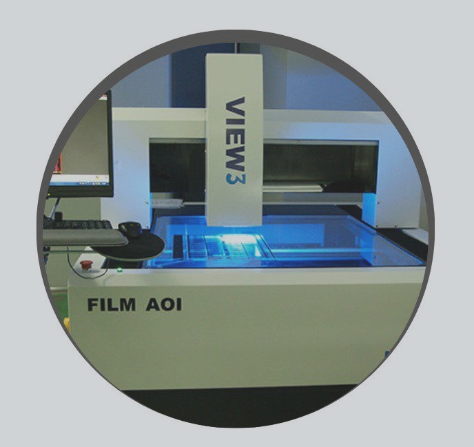
4: Solder mask color: There are various colors available, and you can choose according to requirements, with the standard default being green.
5: Silkscreen color: The color of the text and frame printed on the PCB is typically white by default.
6: Copper thickness: Copper thickness is determined scientifically based on the PCB circuit’s current requirements; thicker copper foil increases production costs.
7: Whether vias are covered by solder mask: Solder mask is applied to insulate vias; otherwise, they remain uninsulated.
8: Surface treatment: Primarily serves as an anti-oxidation measure; the standard default treatment is tin spray coating.
9: Production quantity determines the production cycle and cost: Higher quantities lead to lower prices but longer production times, while smaller quantities incur higher costs but shorter production times.
Certainly! Here’s the revised and polished version of the text:
—
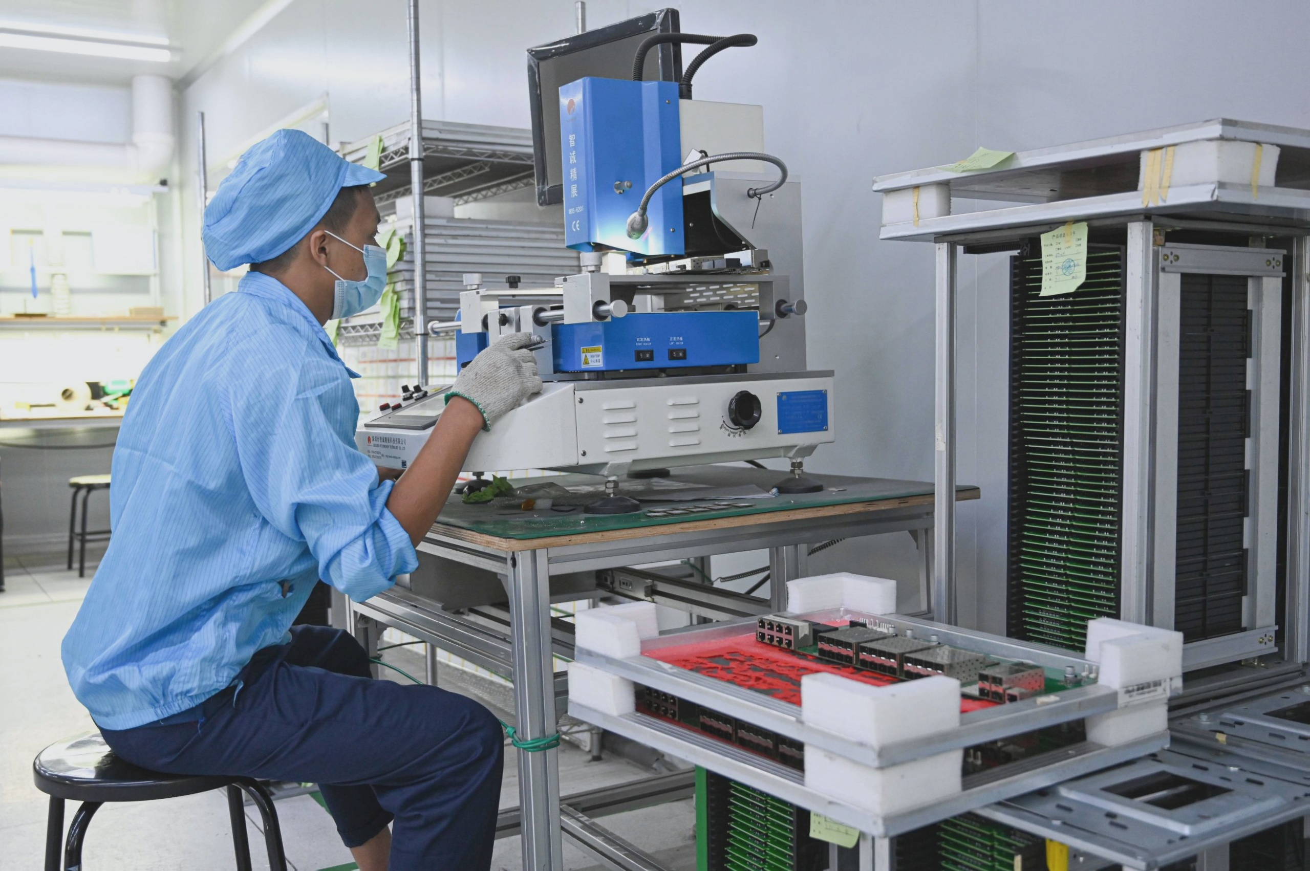
Small batch PCB manufacturers are specialized processing plants that excel in fast prototyping cycles. Their major advantage lies in rapid turnaround times, allowing urgent orders to be prioritized and seamlessly integrated into production queues—an efficiency typically unmatched by larger facilities. Below, we introduce several crucial processes involved in the operations of small batch PCB manufacturers:
1. **Drilling:** This process involves creating holes in the PCB for wiring connections. Via punching is essential for establishing circuit connections, while structural requirements dictate hole placement for positioning and other purposes. In multi-layer boards, holes are not uniformly drilled; some are buried within the circuitry, while others are exposed on the board’s surface.
2. **Solder Mask:** Also known as solder resist, this refers to the protective layer applied to PCBs to insulate and shield areas that do not require soldering. It is commonly recognized by its green color.
3. **Openings (or “Open Windows”):** These are sections of the PCB where the solder mask is intentionally omitted. These exposed areas are crucial for facilitating soldering and ensuring electrical connections.
4. **Tin Plating:** This surface treatment involves applying a thin layer of tin to exposed copper areas of the PCB. Tin plating serves to protect the copper from oxidation and corrosion, as well as to facilitate soldering during assembly.
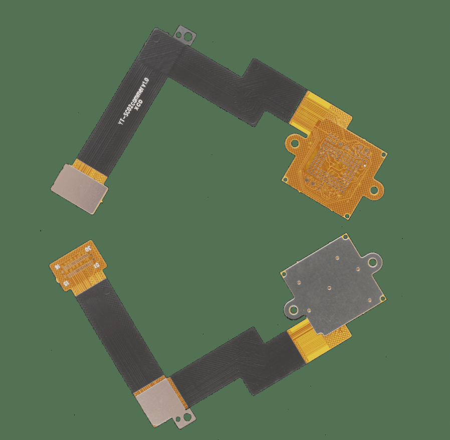
Silk screen: The silk screen layer, positioned atop the PCB, serves primarily for textual annotations. It facilitates circuit installation and maintenance by imprinting necessary logos, patterns, and text codes on both the upper and lower surfaces of the board.
SMOBC: SMOBC (Solder Mask Over Bare Copper) refers to the process where solder mask is applied directly over treated copper surfaces. This approach contrasts with methods where copper is coated with mask before treatment.
Mesh plate: A mesh plate, also known as wire mesh, steel mesh, or copper mesh, is essential for solder paste printing in Surface Mount Technology (SMT). Its purpose is to apply solder paste accurately onto the PCB for subsequent component placement and reflow soldering. Upon receiving customer specifications, PCB manufacturers verify the mesh against the solder layer to ensure proper alignment and the absence of any leakage windows, then proceed with stencil production.
Testing: Manual Visual Testing is a widely employed method for in-circuit testing. It involves visual inspection by human operators to verify component placement on the PCB through direct comparison and visual examination.

