PCB Design Elements and Specifications
The composition of relevant design elements in the PCB should be clearly defined within the design specification. The shape is represented by mechanical layers 1 to 16 (in order of priority) or a no-entry layer. When both are used in the PCB design file, a common shielding layer can be employed to disable routing, rather than opening holes. The machine layer 1 should be used for molding. In the PCB design drawing, a long slot or cutout should be shown, with the corresponding shape drawn on the “mechanical 1” layer.
Important Considerations for PCB Design
- Overall Dimension Tolerance: The size of the PCB must adhere to the design specifications. If no specific dimensions are provided, the dimensional tolerance should be ±0.2mm.
- Flatness (Warpage) 0.7%: Understanding the concept of stratification is crucial for PCB design. Different layer configurations impact how signals and components are arranged on the board.
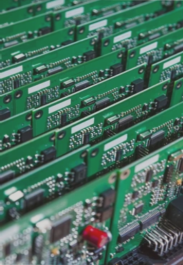
Printed Traces and Pads
When designing PCB layouts, it’s essential to consider various factors to ensure optimal performance and manufacturability.
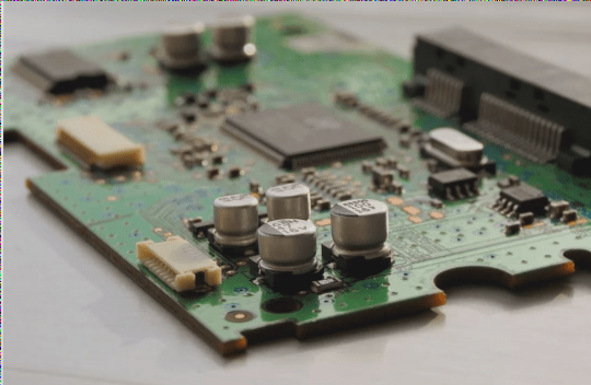
PCB Layout Guidelines
- Trace Width and Spacing: The layout, trace width, and spacing of printed conductors and pads should meet design requirements. Adjustments may be necessary based on process specifications to enhance soldering reliability.
- Through-Hole Design: For through-holes (VIA), specific diameter considerations should be made to ensure proper functionality.
- Tin-Plating and Gold-Plating: Different plating processes require specific trace width and spacing designs for optimal production outcomes.
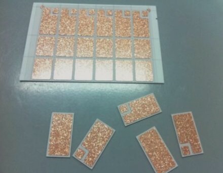
- Grid Processing: Using a grid pattern for large copper areas can help prevent blistering and thermal stress during PCB bending.
- Heat Shield (Thermal Insulation Pad): Designing pads with electrical and process considerations in mind can improve soldering outcomes.
- Inner Traces & Copper Isolation: Proper insulation and distance considerations are crucial to avoid short circuits and ensure the integrity of the PCB.
If you have any PCB manufacturing needs, please feel free to contact us.