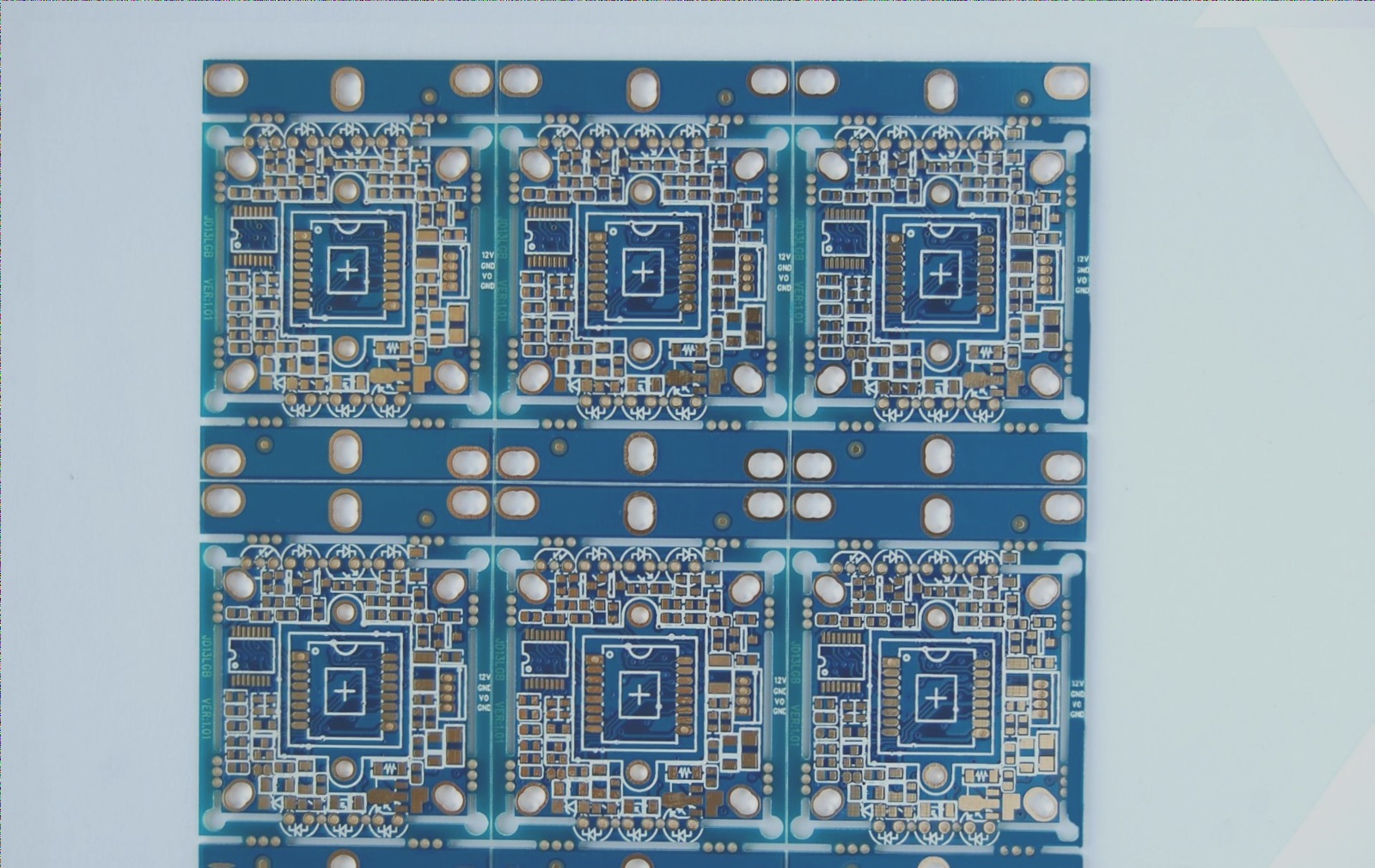
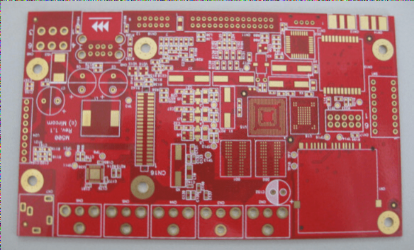
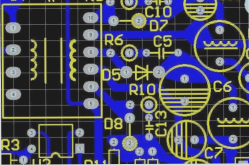
Make sure that the signal line is as short as possible during PCB layout. When the length of a signal trace exceeds 300mm, a parallel ground trace must be placed. Ensure minimal loop area between signal lines and their corresponding returns. For longer traces, alternate the positions of signal and ground traces every few centimeters to minimize loop area. Drive signals from the center of the network to multiple receiving circuits. Minimize the loop area between power supply and ground, and place high-frequency capacitors close to each IC power pin. Position high-frequency bypass capacitors within 80mm of each connector. Where feasible, fill unused areas with ground planes, connecting all ground fills across layers every 60mm. Ensure that opposite ends of any large ground fill (approximately >25mm x 6mm) are connected to ground. Use narrow traces to bridge gaps exceeding 8mm on power or ground planes. Keep reset, interrupt, and edge-triggered signal traces away from PCB edges. Connect mounting holes to common ground or isolate them. (1) Use zero-ohm resistors when metal brackets require connection to shielding devices or chassis. (2) Determine mounting hole sizes for reliable installation of metal or plastic brackets. Use large pads on top and bottom layers of mounting holes, avoiding solder resist on bottom pads and ensuring they avoid wave soldering. Do not route protected and unprotected signal traces in parallel. Pay special attention to routing reset, interrupt, and control signal traces during PCB layout. (1) Implement high-frequency filtering. (2) Maintain separation from input/output circuits. (3) Keep away from PCB edges.

The PCB proofing should be inserted into the enclosure rather than being placed in an exposed position or internal seam. Attention should be paid to the wiring beneath the magnetic beads, as well as the contact points between the pads and the signal lines, which may come into contact with the magnetic beads. Some magnetic beads exhibit high conductivity and could create unexpected conductive paths.
When multiple PCB boards are housed within a chassis or motherboard, the board most sensitive to static electricity should be positioned in the center.
Regarding PCB etching, differences exist between the upper and lower surfaces of the boards, as well as between the leading and trailing edges. Many issues related to etching quality are concentrated on the upper board surface due to adhesive-like clumps left by the etchant. The buildup of these colloidal slabs on the copper surface affects spray coverage and impedes the replenishment of fresh etching solution, thus slowing down the etching process.
The formation and accumulation of colloidal slabs lead to varying degrees of etching between the upper and lower patterns of the board. Consequently, the initial section of the board in the etching machine may be etched completely or overly corroded due to faster etching speeds before accumulation occurs. Conversely, sections following the initial part already experience slowed etching speeds due to existing accumulation.
Maintenance of PCB etching equipment is crucial. Ensuring the cleanliness and unobstructed flow of the nozzles is paramount to maintaining uniform etching. Nozzle clogging or slagging can result in uneven etching, potentially rendering the entire PCB unusable. Regular maintenance involves replacing worn or damaged parts, including the nozzles themselves, which are prone to wear.
Moreover, preventing slagging buildup within the etching machine is critical. Accumulated slag can disrupt the chemical balance of the etching solution, leading to further operational issues. Addressing excessive slag accumulation promptly is essential, often requiring thorough cleaning with strong hydrochloric acid or adjusting the solution balance accordingly.


