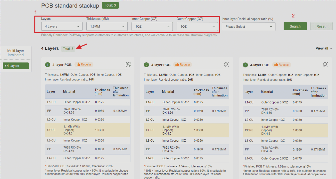
PCB Layout Principles for Circuit Board Proofing
- Consider the distribution parameters of circuit components under high-frequency operating conditions to arrange components uniformly, neatly, and compactly on the double-sided PCB.
- Physically separate analog and digital circuits to prevent signal interference.
- Strategically place the clock circuit at the center of the PCB with proper grounding.
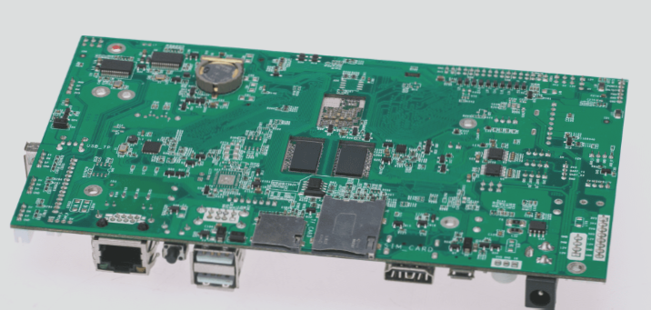
Designing the Optical Burst Module Circuit
- Position the laser MAX3656 and associated components according to SFMSA specifications.
- Place the limiting amplifier, MAX3747, close to the main amplifier chip, MAX3748, to ensure accurate signal reception and minimize interference.
- Centrally locate the clock and data recovery circuit, MAX3872, with a reliable ground connection.
- Utilize the MAX3654-47-870MHz analog CATV inter-block amplifier for integrated processing.
Controlling PCB Cost
- Consider the number of PCB layers to balance cost and performance.
- Optimize PCB size to reduce costs without compromising performance.
- Ensure manufacturing ease by setting reasonable parameters for line width, spacing, and hole sizes.
- Choose cost-effective materials like RF4 to keep production costs down.
If you require PCB manufacturing services, feel free to contact us.