PCB Design Flow: Prototyping and Product Development
Prototyping:
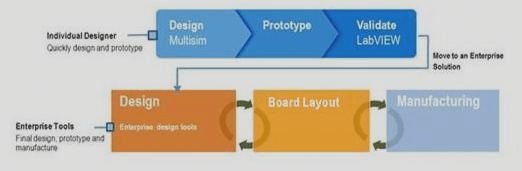
Prototyping is a crucial initial stage in PCB design flow. Engineers conduct research to define the application for which the PCB is intended. The design must align with the application, ensuring accuracy and efficiency while conserving time and resources. Minimizing the number of prototypes saves time and resources. Once the prototype design is confirmed, it progresses to the next stage: product development.
Product Development:
Product development involves implementing the PCB prototype to create the final PCB for its intended application. Companies often engage in mass production of PCBs, emphasizing the use of prototypes that optimize resources and maximize yield.
Both stages, prototyping and product development, require distinct tools and processes. Research plays a vital role in product development, enabling designers to create products efficiently without needing expertise in simulation, layout, or schematic capture. The ability to define circuit schematics quickly, validate circuit behavior using advanced analysis techniques, transfer schematics to layouts seamlessly, and verify the design’s behavior are essential skills for researchers.
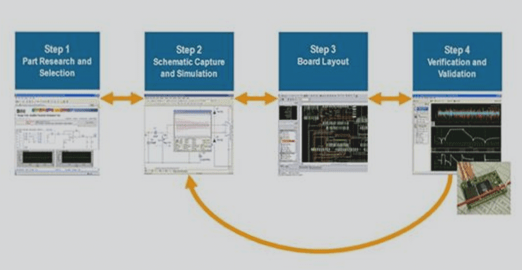
1: Research & Selection
Central to PCB prototyping is the selection of components for the design. Semiconductors, including those from Analog Devices, National Semiconductor, NXP, Rohm, Linear Tech, and Texas Instruments, are fundamental materials. Engineers can research semiconductor performance, utilize manufacturer web resources, and simulation tools to evaluate components effectively.
2: Schematic Capture and Simulation
Schematic capture involves creating the electronic circuit diagram, representing components like capacitors, resistors, and amplifiers with symbols. This step aids in viewing the circuit theoretically and is crucial for simulation using tools like SPICE (Simulation Program with Integrated Circuit Emphasis), PSpice, and HSpice to ensure circuit integrity and error detection.
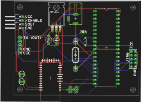
3: Board Layout
PCB Design Process: From Schematic to Prototype
Step 1: Schematic Design
Once the schematic design is complete, it is time to transfer it to a board layout. Each symbol in the schematic corresponds to a land pattern, which is crucial for attaching and connecting components to the PCB.
Step 2: Board Layout
In this stage, the board outline is defined, components are placed, copper connections are established, and the board is prepared for fabrication.
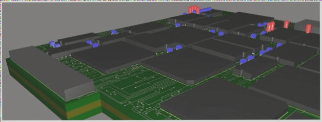
Step 3: Verification & Validation
After fabrication, the board undergoes validation through prototype tests to ensure it meets the original specifications. Once validated, the prototype progresses to the product development stage.
Benefits of Prototyping
- Prototyping saves time and money.
- It helps test innovative ideas and eliminate unsuccessful approaches early on.
- Prototyping aids in gathering accurate project requirements.
- Identifying technical issues in the design for better accuracy.
- Allows testing of different feature implementations for optimal results.
- Prototypes demonstrate idea feasibility and increase chances of funding.
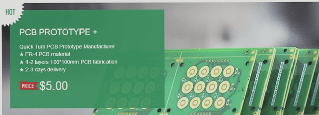
Explore wellcircuits for Quick Turn PCB Fabrication and PCB Assembly