1. **PCB Copy Board Layout**
The positioning of components related to the mechanical size of power sockets, switches, inter-PCB interfaces, indicators, and other elements is crucial and should align with the mechanical dimensions of the positioning components. Typically, the interface for power supply connections is placed along the PCB edge, around 3mm to 5mm away from it. Light-emitting diodes (LEDs) should be positioned precisely according to specific requirements. Switches and fine-tuning components, such as adjustable inductors and resistors, should be placed near the PCB edge to facilitate easy adjustment and connection.
Components that are likely to require frequent replacement should be located in areas with minimal surrounding equipment to simplify the replacement process.
High-power components, such as transistors, transformers, and rectifiers, which generate significant heat under high-frequency conditions, must be considered carefully during the layout phase. Ventilation and heat dissipation are critical for these components. They should be placed in areas that allow for adequate airflow around the PCB.
High-power rectifiers and regulation tubes should be fitted with heatsinks and positioned away from transformers. Similarly, components sensitive to heat, such as electrolytic capacitors, should be kept distanced from heat-generating parts to prevent drying out of the electrolyte, which can lead to increased resistance and poor performance, ultimately compromising the circuit’s stability. Additionally, it is important to plan for components prone to failure, such as regulation tubes, electrolytic capacitors, and relays, in easily accessible locations for maintenance and replacement.
1. For test points that require frequent measurements, it is important to ensure easy access for the test probe when arranging components. A leakage magnetic field at 50 Hz is generated inside the power supply device. When the low-frequency amplifier is connected to specific parts of the power supply, it may cause interference. To avoid this, they must be either separated or shielded. The amplifiers at various stages should be arranged in a straight line according to the schematic diagram. The benefit of this approach is that ground currents at all levels are enclosed and flow at their respective levels without affecting the operation of other circuits.
2. The input and output levels should be kept as far apart as possible to minimize parasitic coupling interference. Considering the signal transmission relationships between the functional circuits, low-frequency and high-frequency circuits should be kept separate, and analog circuits should be isolated from digital circuits. The integrated circuit should be placed centrally on the PCB to allow easy connections between each pin and the wiring of other components. Inductors, transformers, and similar components, which exhibit magnetic coupling, should be positioned orthogonally to one another to reduce such coupling.
3. Additionally, since these components generate strong magnetic fields, sufficient space or magnetic shielding should be provided around them to minimize their impact on other circuits. High-frequency decoupling capacitors should be placed strategically on the PCB. For instance, a 10μF–100μF electrolytic capacitor should be used at the PCB power input, while a 0.01μF ceramic chip capacitor should be placed near the integrated circuit’s power supply pin.
4. Certain circuits may require appropriate high-frequency or low-frequency chokes to mitigate interference between high- and low-frequency circuits. This consideration should be incorporated during the schematic design and layout stages, as neglecting it could adversely affect the circuit’s performance. Components should be spaced appropriately, taking into account the possibility of penetration or emission between them.
5. For amplifiers using push-pull or bridge circuits, it is crucial to maintain symmetry in both the electrical parameters of the components and the layout structure to ensure that the distribution parameters remain as consistent as possible. Once the main components are manually placed, component locking methods should be used to prevent them from shifting during automatic layout. In other words, the Editchange command or a lock on the component properties should be applied to secure them in place.
6. For common components such as resistors and capacitors, the layout should prioritize neatness, minimized floor area, efficient wiring, and ease of soldering. This will allow the board layout to be automatically read and optimized.
7. **Selecting PCB Components**
Starting with safety design requirements, safety-critical components containing dangerous voltages, such as 220V power sockets, fuses, and power modules, must meet safety certifications (e.g., 3C certification in China). For other non-safety-critical components, surface-mount SMT devices are generally preferred over through-hole TTL dual-row in-line components, provided they meet the price and functionality requirements.
8. When choosing components for IC circuits, power and switching speed should be considered. Higher IC power and faster switching speeds are generally better, as long as the reliability requirements are met. However, it’s important to recognize that there are trade-offs, such as sensitivity and anti-interference, which need to be balanced to achieve the optimal design.
9. Resistors, capacitors, and inductors can generally be selected as SMT components, with large-capacity capacitors possibly being considered in other forms. Component selection should prioritize functionality, while also adhering to the three “reductions” principle:
1. Reduce IC circuit switching speeds to minimize harmonic components.
2. Minimize working current and power consumption.
3. Reduce circuit area.
SMT components are often the best choice due to their small size, high integration, and reliability.
10. **Test Results and Radiation Considerations**
Figure 7 shows the test results for three different devices assembled on the same PCB. Among these, the SMT option exhibits the lowest radiation.
11. **Summary**
When selecting components, it is not about choosing the highest power or the fastest speed but about meeting the design requirements using compatible indicators and minimizing costs. The goal is to achieve the optimal design combination, which may vary depending on the type and grade of the device.
12. **PCB Design and Routing**
Before routing on the PCB, it is crucial to understand the potential issues related to power supply, ground interference, and radiation. During operation, the transient currents in the power supply and ground can introduce inductive and capacitive effects, leading to noise and interference, as shown in Figure 8, which illustrates the voltage and current waveforms for power (VCC, ICC) and ground (IG, VG). This interference becomes especially problematic when multiple circuits are active.
13. For complex PCBs, a four-layer design is recommended. This allows signal routing on the top and bottom layers, freeing up more space and, more importantly, providing a low-impedance ground layer and power plane, particularly the ground plane, which significantly reduces the loop area and ground impedance for IC circuits. Typically, the top layer is used for signal lines, the second layer for DC ground, the third layer for DC power, and the fourth layer for additional signal lines.
14. When the PCB includes both logic and analog circuits, their ground connections should be isolated (with isolation width > 3mm). Methods like short-circuiting or using magnetic beads can ensure they share the same potential reference. In cases where numerous logic and analog circuits are present, power and ground areas must be carefully managed, and the coupling between IC circuits should be minimized by considering the principle of reducing current flow area.
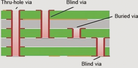
15. To maintain low ground impedance, a dual-layer ground design should be used, with horizontal and vertical grounding wires forming a grid. These should be connected by metalized vias, ensuring that each IC chip has a dedicated ground wire. Ground wires should be placed every 1-15 cm to make them dense, reducing signal loop area and minimizing radiation.