1. A PCB copy board, also known as a circuit board copy, raises the question: what exactly is a circuit board, and what constitutes a PCB copy board? Additionally, what is the relationship between the circuit schematic, the circuit board, and the PCB copy board?
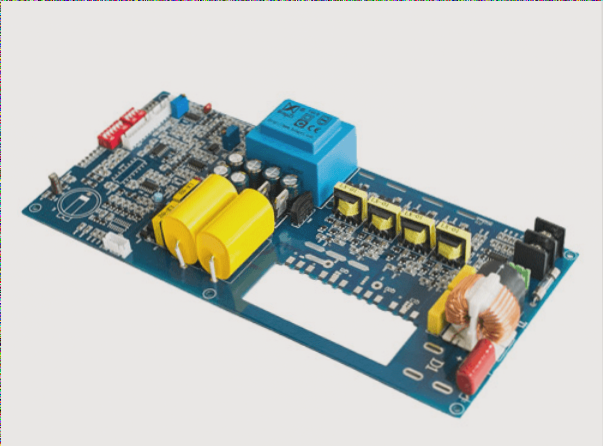
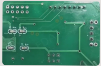
2. In technical terms, a circuit board is an insulating substrate on which components such as pads, vias, copper traces, text markings, and mounting holes are positioned. The component pins are soldered to the circuit board through the pads. The connections between the various parts are made via copper traces, and the mounting holes are used to secure the board in place with bolts.
3. A circuit board consists of an insulating substrate with a conductive copper layer covering its surface, and the copper layer serves to establish electrical connections. In the past, circuit board substrates were primarily made from bakelite, but today, epoxy resin boards are more commonly used. The current trend shows a shift towards thinner boards, greater toughness, and an increase in the number of layers.

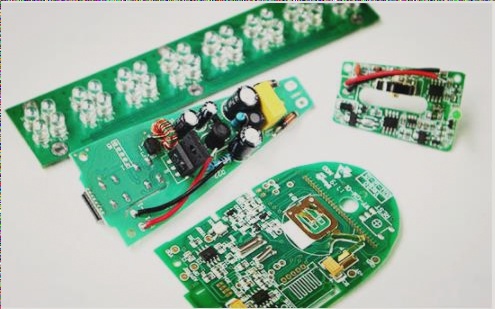
1. Based on the wiring level of the circuit board, it can generally be categorized into three types: single-layer boards, double-layer boards, and multi-layer boards. For multi-layer boards, the manufacturing technology for 4-layer boards is well-established, while circuit boards with 6 or more layers are typically used only in advanced equipment due to their complex manufacturing process and high cost. However, with continuous technological advancements, circuit boards with up to nearly 30 layers are beginning to see applications in some industries.
2. Understanding the circuit board leads us to understand the circuit schematic diagram. A circuit schematic refers to a drawing that illustrates the electrical connections between components within the circuit. It does not specify the size or shape of the components but focuses on their types and the electrical connections between them. Circuit schematics typically include two main elements: electrical components and their interconnections. Electrical components are the primary elements in the schematic, including resistors, capacitors, diodes, operational amplifiers, etc. In the schematic, these components are represented by their symbols, component IDs, and values, but without details such as the physical shape, size, pad spacing, or pad positions of the components. Such information is usually provided in the circuit layout (PCB diagram). The interconnections in the schematic are represented by wires linking the electrical nodes of each component, showing the electrical relationships between them and reflecting the designer’s design intent.
3. Circuit boards and circuit schematics are closely related to PCB reverse engineering. PCB reverse engineering refers to the process of analyzing a physical electronic product and its circuit board through reverse research and development techniques. This process allows for the extraction of the original PCB files, Bill of Materials (BOM), schematic diagrams, and other technical documents for 1:1 replication. These technical files are then used to manufacture the PCB, assemble components, perform flying probe testing, and debug the circuit board, ultimately resulting in a complete copy of the original circuit board. Since electronic products consist of various types of circuit boards that control different functions, the PCB reverse engineering process can be used to extract the full technical data of any electronic product and replicate or clone the product.
4. From the definition above, it is clear that PCB reverse engineering is the process of reverse design for circuit boards, as well as the reverse analysis of circuit schematic diagrams. This is because an existing circuit board is initially designed based on a circuit schematic, which defines the layout and connections. On the other hand, PCB reverse engineering starts with a designed and implemented circuit board, which is then reverse-analyzed to derive the PCB layout files and the corresponding schematic diagram. This process involves examining the interconnections and dependencies among the components, the PCB layout, and the schematic diagram.
2. In technical terms, a circuit board is an insulating substrate on which components such as pads, vias, copper traces, text markings, and mounting holes are positioned. The component pins are soldered to the circuit board through the pads. The connections between the various parts are made via copper traces, and the mounting holes are used to secure the board in place with bolts.
3. A circuit board consists of an insulating substrate with a conductive copper layer covering its surface, and the copper layer serves to establish electrical connections. In the past, circuit board substrates were primarily made from bakelite, but today, epoxy resin boards are more commonly used. The current trend shows a shift towards thinner boards, greater toughness, and an increase in the number of layers.

1. Based on the wiring level of the circuit board, it can generally be categorized into three types: single-layer boards, double-layer boards, and multi-layer boards. For multi-layer boards, the manufacturing technology for 4-layer boards is well-established, while circuit boards with 6 or more layers are typically used only in advanced equipment due to their complex manufacturing process and high cost. However, with continuous technological advancements, circuit boards with up to nearly 30 layers are beginning to see applications in some industries.
2. Understanding the circuit board leads us to understand the circuit schematic diagram. A circuit schematic refers to a drawing that illustrates the electrical connections between components within the circuit. It does not specify the size or shape of the components but focuses on their types and the electrical connections between them. Circuit schematics typically include two main elements: electrical components and their interconnections. Electrical components are the primary elements in the schematic, including resistors, capacitors, diodes, operational amplifiers, etc. In the schematic, these components are represented by their symbols, component IDs, and values, but without details such as the physical shape, size, pad spacing, or pad positions of the components. Such information is usually provided in the circuit layout (PCB diagram). The interconnections in the schematic are represented by wires linking the electrical nodes of each component, showing the electrical relationships between them and reflecting the designer’s design intent.
3. Circuit boards and circuit schematics are closely related to PCB reverse engineering. PCB reverse engineering refers to the process of analyzing a physical electronic product and its circuit board through reverse research and development techniques. This process allows for the extraction of the original PCB files, Bill of Materials (BOM), schematic diagrams, and other technical documents for 1:1 replication. These technical files are then used to manufacture the PCB, assemble components, perform flying probe testing, and debug the circuit board, ultimately resulting in a complete copy of the original circuit board. Since electronic products consist of various types of circuit boards that control different functions, the PCB reverse engineering process can be used to extract the full technical data of any electronic product and replicate or clone the product.
4. From the definition above, it is clear that PCB reverse engineering is the process of reverse design for circuit boards, as well as the reverse analysis of circuit schematic diagrams. This is because an existing circuit board is initially designed based on a circuit schematic, which defines the layout and connections. On the other hand, PCB reverse engineering starts with a designed and implemented circuit board, which is then reverse-analyzed to derive the PCB layout files and the corresponding schematic diagram. This process involves examining the interconnections and dependencies among the components, the PCB layout, and the schematic diagram.


