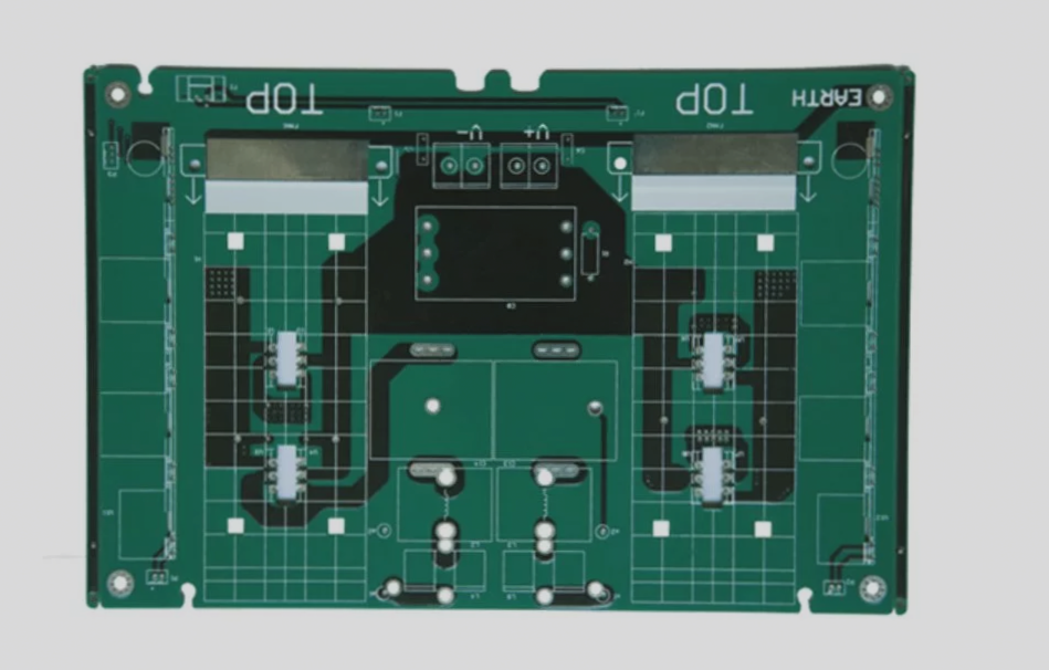
RF Circuit PCB Design
Advancements in RF Circuit Design for Handheld Devices
As communication technology progresses, RF circuitry plays a vital role in devices like wireless pagers, mobile phones, and wireless PDAs. The quality of these devices heavily relies on the performance of RF circuits. Miniaturization is a key feature, leading to high component density and significant interference between components. Handling EMI signals improperly can disrupt the entire circuit system. Thus, preventing and suppressing EMI while enhancing EMC is crucial in RF circuit PCB design. The design structure of the PCB greatly influences the circuit’s performance metrics.

Key Strategies for RF Circuit PCB Design
- 1. Component Placement and Circuit Segregation:
- 2. Wiring Principles and Signal Integrity:
- 3. Ground Line Management:
- 4. Minimizing Radiation and Enhancing Reliability:
Determine the position of interface components on the PCB and their connections with other boards or systems. Emphasize the coordination and orientation of components, especially in compact handheld devices. Prioritize the placement of larger components and analyze the circuit structure in blocks to segregate signals effectively.
Focus on maintaining low-density wiring and appropriate sizing of signal traces for impedance matching. Pay meticulous attention to signal line direction, width, and spacing to avoid cross-interference. Optimize power traces and minimize trace lengths and via counts for enhanced anti-interference capabilities.
Divide ground lines into sections, separate digital and analog ground lines, and follow single-point grounding principles to reduce interference. Connect ground lines to power ground separately and isolate modules with dedicated ground lines to prevent signal coupling.
Focus on layout and wiring strategies to minimize radiation and improve anti-interference capabilities. These methods enhance electromagnetic interference performance and achieve electromagnetic compatibility, crucial for integrating wireless communication functions into electronic products.
Professional RF Circuit PCB Design for IoT Integration
With the rise of IoT technologies, the integration of wireless communication functions into electronic products through RF circuit PCBs demands professional design and simulation tools. A well-executed design ensures reliability and optimal performance in modern communication devices.