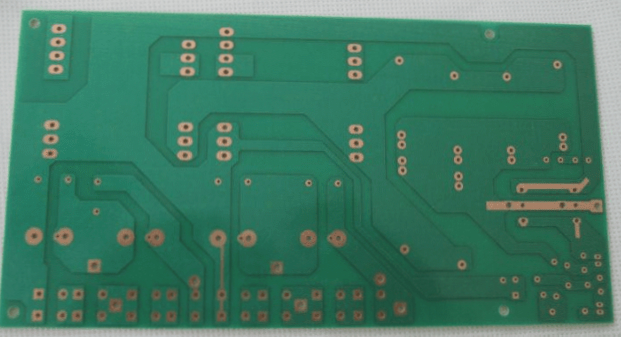
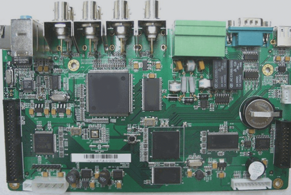
Sometimes, the production process of printed circuit boards may seem very complicated. WellCircuits Limited will provide you with an analysis of the production process of printed circuit boards. First and foremost, it is essential to understand the function and role of printed circuit boards. The primary purpose of these boards is to serve as a base for the assembly of electronic circuit parts to create a module or finished product with specific functionalities. Therefore, the printed circuit board process is utilized in various electronic products, ranging from electronic watches, computers, communication equipment, to military weapon systems. As long as there are electronic components like integrated circuits requiring electrical interconnection, printed circuit boards are indispensable.
The production process of printed circuit boards is typically categorized into three types: single-layer, double-layer, and multi-layer boards. Although different factories may use varying terminology, the fundamental principle of the process flow remains consistent.
The production process for single-layer boards is relatively straightforward compared to double-layer boards. It involves cutting, drilling, transferring graphics, etching, applying solder mask and printing, metal surface treatment, final product molding, testing, inspection, and packaging for shipment.
In contrast, the production process for double-sided boards includes cutting, drilling, electroless copper plating, copper plating, transferring graphics, pattern plating, applying protective tin plating, etching, intermediate inspection, solder mask application, character printing, metal surface treatment, final product molding, electrical testing, appearance inspection, and packaging for shipment.
The multi-layer board production process incorporates an additional inner layer process before the double-layer process. It includes cutting, inner layer graphics transfer, inner layer etching, inspection, copper surface oxidation treatment, typesetting, lamination board, pressing board, cutting board forming, followed by the double-sided board process.
The evolution of printed circuit board production has progressed from single-layer to double-layer and multi-layer boards, each maintaining its development trajectory. With a continual focus on high precision, high density, space reduction, cost-effectiveness, and enhanced utilization in future electronic equipment development, printed circuit boards will continue to display robust vitality.


