Understanding PCB Openings and Tin Plating in Design
- What are PCB Solder Mask Openings?
- Utilizing Openings and Bright Copper
- The Role of Tin Plating in PCB Wiring
- Setting Opening Steps in PCB Design
In PCB design, solder mask openings are crucial for exposing copper traces for tin plating, enabling proper soldering of components and preventing short circuits.
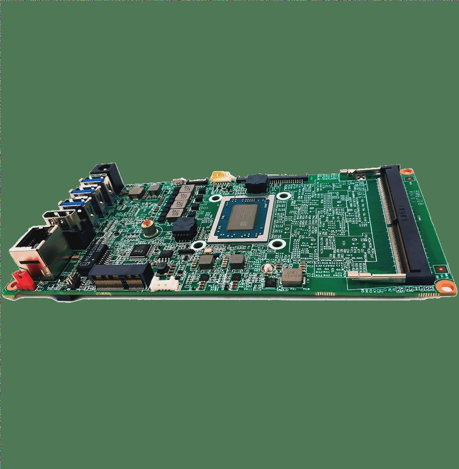
Openings and bright copper in PCB design are essential for enhancing current-carrying capacity, thermal dissipation, and functionality, especially in power supply and motor control boards.
Tin plating plays a vital role in enhancing solderability, protecting copper surfaces from oxidation, and ensuring reliable solder joints in PCB manufacturing.
Properly setting opening steps involves precise removal of solder mask, correct dimensions for openings, and alignment with design specifications to meet functionality and manufacturability requirements.
Effective communication with customers and clear design specifications are key to avoiding misunderstandings and ensuring that PCB designs meet technical requirements.
Additional Insights:
- 1. Shielding
- 2. Solder Mask Openings
When adding shielding to PCB designs, ensure the solder mask width is at least 1 mm, expand network copper within masked areas, and provide complete coverage to prevent substrate exposure.
Properly placed solder mask openings are essential for facilitating component soldering and enhancing the overall reliability and functionality of PCBs.
PCB Design Tips for Enhanced Performance
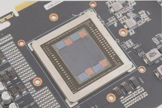
- Vias and Solder Mask Openings: When dealing with PCB vias or holes, especially in BGA-based designs, it’s crucial to consider the hole size. Holes larger than 12 mils should have solder mask openings to facilitate effective soldering and prevent solder bridging.
- IC Thermal Pads: For ICs requiring thermal management, ensure the solder resist pad is larger than the surface pad to aid in heat dissipation. Connect ground holes on the IC’s thermal pad to a copper-clad solder mask for improved heat transfer across the PCB.
- Solder Touch (Wave Soldering): Address soldering challenges caused by close pad spacing by modifying pad shapes and incorporating scratch pads. Matching copper bumps to the solder mask size can enhance soldering quality and prevent defects.
- PCB Trace Current Handling: Widening current-carrying traces and removing solder mask from the current path can better manage large current spikes, especially in relay-driven circuits. Tin plating post mask removal can further boost current-carrying capacity.
- Enhanced Current Capacity Implementation: Draw current-carrying traces on the top or bottom layer, ensuring alignment with the corresponding solder mask layer to improve current handling capabilities.
- Defining Solder Mask Openings: Utilize TOP/BOTTOM SOLDER layers to create solder mask openings for pads, vias, and non-electrical traces. Properly configured solder mask openings are vital for wave soldering and component soldering.
By following these guidelines and optimizing solder masks, thermal pads, and current handling, you can significantly boost your PCB’s reliability, manufacturability, and overall performance.