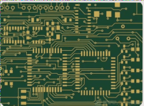
PCB Stack-Up Design Guidelines
In general, PCB stack-up design follows two key rules:
- Each trace layer must have an adjacent reference layer, either a power or ground layer.
- Maintain a minimum distance between the adjacent power layer and ground layer to provide sufficient coupling capacitance.
Example: Stack-Up Design from Two-Layer to Eight-Layer PCB
I. Stack-Up for Single-Sided and Double-Sided PCBs
For two-layer boards, lamination is not a concern due to the small number of layers. The primary consideration for controlling EMI radiation is the routing and layout of traces.
The electromagnetic compatibility (EMC) issues in single-layer and double-layer boards become more prominent as the signal loop area increases. This not only generates strong electromagnetic radiation but also makes the circuit more susceptible to external interference. The simplest way to improve EMC is to minimize the loop area of critical signals.
Critical Signals: These are signals that either generate strong radiation (such as low-order clock or address signals) or are sensitive to external interference (typically low-level analog signals).
Single and Double-Layer Boards for Low-Frequency Analog Designs (< 10 KHz):
- Route power cables in a radial pattern to minimize their total length.
- Keep power and ground traces close to each other. Place a ground trace next to key signal traces to minimize loop area and reduce differential mode radiation sensitivity to external interference. The signal current will naturally follow the shortest loop formed by the signal and adjacent ground traces.
- For double-sided boards, route a ground trace on the opposite side of the signal trace to minimize loop area. The loop area is determined by the board thickness and signal trace length.
II. Stack-Up for Two-Layer and Four-Layer PCBs
- SIG-GND (PWR) – PWR (GND) – SIG
- GND – SIG (PWR) – SIG (PWR) – GND
For the above stack-up designs, potential issues include large layer spacing for a typical 1.6mm (62 mil) board thickness, which can negatively affect impedance control, interlayer coupling, and shielding. The increased distance between power and ground planes can reduce board capacitance and hinder noise filtering.
The first stack-up option is typically used for boards with many chips, providing good signal integrity (SI) performance but less optimal EMI performance. Routing and layout details are key to controlling EMI. Ensure the ground layer is placed adjacent to the signal layer with the densest routing to help absorb and suppress radiation, and consider the 20H rule for board size.
The second stack-up option is suitable for boards with lower chip density and ample space around the chips. In this configuration, the outer layers are ground, and the middle layers are signal/power. A wide power trace ensures low impedance and effective shielding against inner-layer signal radiation, making it ideal for EMI control in 4-layer boards.
Note: Increase the distance between signal and power layers, and orient traces vertically to reduce crosstalk. Maintain proper board size to reflect the 20H rule. When controlling trace impedance, the power and ground layers should be carefully arranged to ensure DC and low-frequency connectivity.
III. Stack-Up for Three-Layer and Six-Layer PCBs
For higher chip density and faster clock frequencies, a six-layer board design should be considered. Recommended stack-ups include:
- SIG-GND-SIG-PWR-GND-SIG: This stack-up provides excellent signal integrity as the signal layers are adjacent to ground layers, and power and ground planes are paired. This configuration controls trace impedances well and ensures proper return paths for signals.
- GND-SIG-GND-PWR-SIG-GND: Suitable for lower-density devices, this stack-up offers the benefits of better shielding with top and bottom ground layers. The power layer should be placed near the non-main component layer to improve EMI performance.
Summary: For six-layer boards, minimizing the distance between power and ground layers improves coupling. Although reducing the layer spacing in a 62 mil board may still be challenging, the second option increases cost significantly. Typically, the first stack-up option is preferred. Follow the 20H rule and mirror layer design guidelines when stacking.
IV. Stack-Up for Four-Layer and Eight-Layer PCBs
The following are three types of stack-ups for four-layer and eight-layer boards:
1. Basic Stack-Up
- Signal 1: Component surface, microstrip routing layer
- Signal 2: Internal microstrip routing layer (X direction)
- Ground
- Signal 3: Stripline routing layer (Y direction)
- Signal 4: Stripline routing layer
- Power
- Signal 5: Internal microstrip routing layer
- Signal 6: Microstrip trace layer
This stack-up is not ideal due to poor electromagnetic absorption and high power supply impedance.
2. Variant with Improved EMI Performance
- Signal 1: Component surface, microstrip routing layer
- Ground layer: Improved electromagnetic absorption
- Signal 2: Stripline routing layer
- Power layer: Improved electromagnetic absorption with the underlying ground layer
- Ground layer
- Signal 3: Stripline routing layer
- Ground layer: High power impedance
- Signal 4: Microstrip trace layer
This variant improves EMI performance by adding a reference layer for better control over the impedance of each signal layer.
3. Optimal Stack-Up
- Signal 1: Component surface, microstrip routing layer
- Ground layer: Superior electromagnetic wave absorption
- Signal 2: Stripline routing layer
- Power layer: Excellent electromagnetic absorption with the underlying ground layer
- Ground layer
- Signal 3: Stripline routing layer
- Ground layer: Enhanced absorption capacity
- Signal 4: Microstrip trace layer
This stack-up method provides the best electromagnetic absorption due to multiple ground reference layers.
Choosing the right stack-up design depends on factors such as the number of signal networks, device density, pin density, signal frequency, and board size. To achieve optimal EMI performance, ensure each signal layer has its own reference layer.
If you have any questions about PCB or PCBA design, please feel free to contact me at info@wellcircuits.com.