Single-Sided PCBs: These basic PCBs concentrate components on one side and wiring on the opposite side (the same side as chip components, with plug-in devices on the other). Because wiring is confined to just one side, this type is termed Single-Sided PCB. Due to their single-sided nature, these PCBs impose strict limitations on circuit design—routes cannot overlap and must navigate around their own paths—making them primarily suitable for early circuitry applications.
Double-Sided PCBs are circuit boards featuring wiring on both sides. However, to enable interconnections between these sides, VIA connections are essential. VIAs are small holes in the PCB filled or coated with metal, facilitating connections between the wiring on both sides. With double the area of single-sided PCBs, they resolve the challenge of complex wiring configurations found in single-sided PCBs by allowing routes to pass through holes to the opposite side. Consequently, double-sided PCBs are better suited for more intricate circuit designs compared to their single-sided counterparts.

—
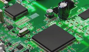
Image 1: GPS Multi-layer PCB
Multilayer PCBs are designed to increase routing area by employing multiple single or double-sided wiring boards. Typically, these boards feature a double-sided inner layer, with two single-sided outer layers or two double-sided inner layers. The printed circuit board is formed by alternating and bonding these layers using positioning systems and insulating materials, interconnecting the conductive patterns according to the PCB’s design requirements, resulting in a 4-layer or 6-layer PCB, commonly known as a multilayer PCB.
The number of layers in a PCB does not necessarily correlate with the number of independent wiring layers; in some cases, additional empty layers are added to control board thickness. Usually, the layer count is even and includes the outermost two layers. While most motherboards consist of 4 to 8 layers, technically, PCBs with nearly 100 layers are feasible.
Many high-performance supercomputers employ multilayer motherboards, although these are increasingly being replaced by clusters of conventional computers. Due to the densely packed layers in PCBs, determining the exact number of layers at a glance is challenging, but close inspection of a motherboard can reveal this information.
—
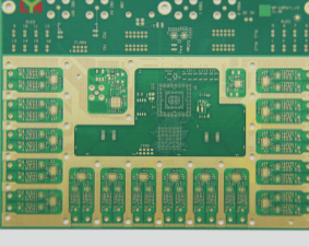
Image 2: Multilayer PCB
Multilayer PCBs exhibit crucial differences that significantly impact their durability and functionality over their lifespan. The following highlights the key characteristics of high-reliability Multilayer PCBs:
1. **Enhanced Reliability:** Improved resistance to z-axis expansion is a notable advantage. However, practical usage may introduce certain risks such as electrical connection issues during soldering or outgassing, challenges during assembly (such as delamination of inner layers or bore wall fractures), and potential failure under operational loads. IPC Class 2 standards (common in most factories) mandate that Multilayer PCBs should have less than 20% copper plating.
2. **Circuit Perfection for Safety:** Ensures reliability and safety without the need for maintenance. Nevertheless, improper repairs can compromise Multilayer PCB integrity. Even with proper repairs, operational stress (like vibration) can lead to potential failures during use.
3. **Enhanced Cleanliness:** Improving the cleanliness of Multilayer PCBs enhances overall reliability. However, there are risks associated with residue accumulation on terminal blocks, solder mask contamination due to accumulated solder, and ionic residues that may cause solder surface corrosion. These issues can result in reliability concerns such as poor solder joints or electrical failures, thereby increasing the likelihood of actual operational failures.
—
This revision addresses clarity and coherence while maintaining the technical details about Multilayer PCBs and their reliability considerations.
Image 3: The solder mask of multilayer PCB
Soldering, Reliability, and Risk of Moisture Intrusion
An unfinished risk arises from the surface treatment of older multilayer PCBs, potentially causing metallographic changes. Moisture intrusion can lead to assembly issues and/or operational problems such as delamination, inner layer separation, and wall failures (open circuits). Whether during manufacturing assembly or real-world use, ensuring the reliable performance of multilayer PCBs is crucial.


