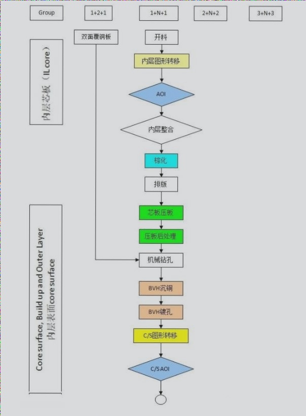
PCB Plating Process Details
- PCB plating process steps include pickling, full board electroplated copper, pattern transfer, acid degreasing, secondary countercurrent rinsing, micro etching, tin plating, pattern copper plating, nickel plating, citric acid treatment, gold plating, and final washing and drying.
- To maintain stability in the sulfuric acid tank solution, it is crucial to remove oxide on the plate surface, activate it, and keep the concentration between 5%-10%.
- The primary copper shield protects freshly deposited thin electroless copper from acid erosion, ensuring uniform surface thickness distribution and effective plating of deep holes and small apertures.
- For PCB full board plating, the current calculation is typically 2 amps per square decimeter multiplied by the platable area of the board.
Additional Considerations in PCB Plating
When working on PCB plating processes, it is essential to:
- Remove oxides on the copper surface of traces and ensure adhesion between primary copper and graphic electroplating.
- Clean the roughened circuit copper surface to guarantee proper adhesion between graphic electroplating copper and primary copper.
- Use sodium persulfate as a micro-etching agent to maintain a stable roughening rate and effective water washing.
- Activate the board surface with a 5%-10% concentration to prevent sulfuric acid tank solution instability.
- Control acid leaching time to avoid surface oxidation and replace acid promptly if needed.
- Achieve a certain thickness of copper for traces and vias to meet the rated current load requirements.
Metal Resist Layer and Tin Electroplating
The metal resist layer, mainly composed of pure tin, is crucial for graphic electroplating to protect the circuit during etching.
- The tin cylinder temperature should be maintained at room temperature, not exceeding 30 degrees Celsius.
- Current calculation for electroplating tin is generally set at 1.5 amps per square decimeter multiplied by the plate’s electroplateable area.
- During summer, consider installing a cooling system for the tin cylinder due to elevated temperatures.
Nickel Plating in PCB Manufacturing
Nickel plating plays a crucial role in PCB manufacturing by acting as a barrier layer between copper and gold layers. This barrier prevents diffusion that could affect solderability and board longevity. Moreover, the nickel layer acts as a primer, enhancing the mechanical strength of the subsequent gold layer.
Process Parameters for Copper Plating
- Use of nickel plating additives
- Management through a 1,000 ampere-hour approach
- Adjustment based on production outcomes
- Addition rate of approximately 200 ml/KAH
Graphic Nickel Plating
Graphic nickel plating is typically calculated at 2 amps per square decimeter. The temperature of the nickel cylinder is maintained between 40-55 degrees Celsius, with an ideal range around 50 degrees Celsius. A heating and temperature control system for the nickel cylinder is necessary.
Gold Plating on Circuit Boards
Gold plating on circuit boards involves both hard gold (gold alloy) and soft gold (pure gold) processes. The hard gold plating tank contains trace metals like nickel, cobalt, or iron. Gold offers characteristics such as good weldability, oxidation resistance, corrosion resistance, low contact resistance, and high alloy wear resistance.
Gold Plating Process
- Gold citrate bath for plating
- Soft gold with gold content around 1 g/L
- pH maintained at approximately 4.5
- Operating temperature at 35 degrees Celsius
- Specific gravity of about 14 Baumé
- Current density around 1 ASD
Maintenance and Protection
Prior to gold plating, a citric acid immersion bath is recommended to reduce contamination risks and stabilize the plating. Rinsing with pure water post-electroplating is crucial for wash-off and recovery, replenishing evaporation losses in the gold tank.