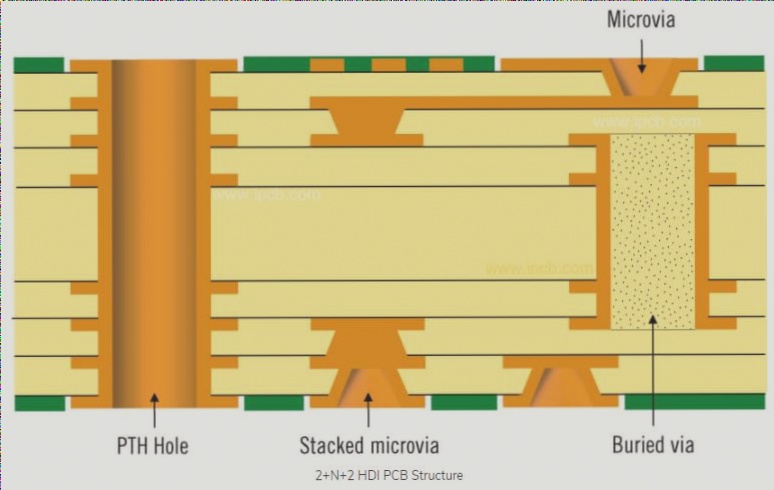
1. VIA, also known as a metalized hole, is one of the critical components in PCB design. In double-sided and multilayer boards, to interconnect the printed wires between layers, a common hole is drilled at the intersection of the wires requiring connection on each layer, known as a via. Blind vias, buried vias, and through vias are the three types of perforations.
2. This article compiles some classic Q&A related to PCB “holes” to provide assistance.
3. **Q:** Should through-holes be minimized in PCB design, and if used, how can their impact on the circuit be reduced?
**A:** For low-frequency signals, through-holes are generally inconsequential, but for high-frequency signals, it’s advisable to minimize their usage. Considering a multilayer board for routing can be beneficial.
4. **Q:** What are the advantages of using blind or buried vias in multilayer board designs?
**A:** Employing blind or buried vias effectively increases the density of multilayer boards, reducing layer count and overall board size while significantly decreasing the number of plated through holes. However, through-holes are more cost-effective in implementation, hence commonly preferred in general designs.
5. **Q:** Is there a simple proportional relationship between plane transport and ring transport simulations in terms of impedance calculations for vias?
**A:** No, the two simulations differ, hence it’s challenging to establish a simple proportional relationship. Online impedance calculation tools specific to vias can aid in maintaining consistent impedance between the via and transmission line.
6. **Q:** What factors affect the maximum allowable current for through-holes in PCBs?
**A:** The copper foil thickness of a typical PCB is around 1 ounce. With a thickness of approximately 1.4 mil, a wire width of 1 mil can typically carry a maximum current of 1A. However, through-hole complexity is influenced by factors such as through-pad size and copper thickness deposited during electroplating.
7. **Q:** Is impedance matching the primary objective when adjusting via parameters?
**A:** Yes, adjusting via parameters aims to achieve better impedance matching, ensuring a smoother impedance transition.
8. **Q:** How does temperature change affect via reliability, and what material selection considerations are relevant?
**A:** Temperature change primarily impacts via reliability, with material coefficient of thermal expansion (CTE) being a critical consideration in material selection.
9. **Q:** In high-speed PCB designs, what approach is recommended regarding the number of vias?
**A:** For high-speed PCBs, it’s advisable to minimize via count and increase the signal layer to fulfill additional routing requirements.
10. **Q:** What are the classifications of PCB through-holes based on function?
**A:** PCB through-holes can be categorized based on function as follows:
1. Signal through-holes (minimizing signal interference)
2. Power supply and ground through-holes (minimizing distribution inductance)
3. Heat dissipation through-holes (minimizing thermal resistance)
Adding grounding through-holes near routing through-holes provides the shortest path for signal return, reducing EMI radiation.
11. **Note:** Signal pass-through layers create impedance discontinuity points, necessitating grounding vias around them to minimize the area of the signal return path and reduce EMI radiation, particularly at higher signal frequencies.
12. **Q:** What challenges arise with small and deep via apertures?
**A:** If the aperture is small and deep, there’s a risk of incomplete metalization.


