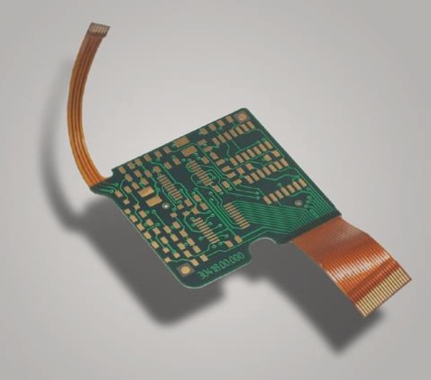
PCB Vias: The Key to Efficient PCB Production
PCB vias are crucial for establishing connections between layers on copper-clad plates. These drilled holes serve the purpose of conduction, enabling electrical connections and securing components.
The Role of Vias in PCB Production
Vias play a critical and irreplaceable role in the production of PCBs. Various processes such as through-hole cover oil, through-hole plug oil, and via window opening are commonly used in PCB fabrication.
- Via Cover Oil: This process involves covering the hole ring of the through-hole with solder mask ink to ensure insulation.
- Via Window Opening: Opening a window through a hole enhances heat dissipation but carries the risk of potential short circuits.
- Via Plug Oil: Filling the through-hole with solder mask ink to prevent solder beads from causing short circuits.
- Resin Plug Via: Coating the via wall with copper, filling the hole with epoxy resin, and coating the surface with copper for enhanced conductivity.
Types of PCB Vias
- Blind Holes: Connect surface and inner circuits with a certain depth on the top and bottom surfaces of PCBs.
- Buried Holes: Connection holes in the inner layers of a circuit board.
- Through Holes: Pass through the entire circuit board and are used for component positioning and installation.
Importance of PCB Via Copper Plating
PCB via copper plating is a crucial step in the manufacturing process, enhancing the board’s strength, durability, and thermal deformation resistance. It also improves power supply performance, signal integrity, and current dissipation ability at connection points.

PCB Via Copper Plating Process
The process of PCB via copper plating involves placing the PCB in a copper plating bath with a sulfuric acid and copper sulfate solution as the electrolyte. Electrodes are added to trigger electrolytic reactions. The current flows through the PCB to evenly coat the through-hole surface with copper. The thickness of copper can be controlled by adjusting current intensity, surface cleanliness, temperature, and hardness before plating.
Benefits of PCB Via Copper Plating
- Thicker and more delicate tin layer on the PCB surface
- Connects the board to the power supply
- Increases power supply stability
- Transmits signals to wireless components
- Improves signal transmission performance
- Enhances power efficiency
Function of PCB Via
A via is a small metal conductor in PCB design that connects components and allows current to pass through.
Advantages of Vias:
- Simplifies the circuit design
- Improves signal transmission
- Enhances packaging density
- Reduces manufacturing costs
- Increases design flexibility
- Improves circuit reliability
In PCB design, vias play a crucial role in connecting components, simplifying circuits, enhancing signal transmission, reducing costs, and improving design flexibility and reliability.