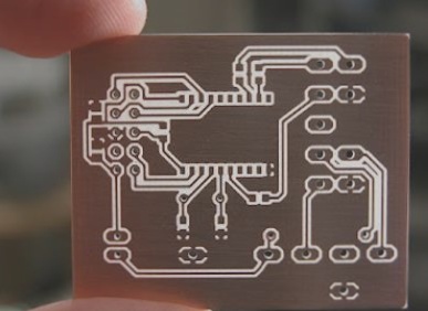
1. How to calculate PCB design line width and current?
2. There are many calculation formulas available on the Internet, but in actual design, it is essential to consider the overall size of the PCB comprehensively.
3. The appropriate line width should be selected based on the current that will pass through the PCB.

The calculation method is as follows: First, calculate the cross-sectional area of the track. The copper foil thickness of most PCBs is 35 μm; multiplying this by the line width gives the cross-sectional area, which should be converted to square millimeters. Use an empirical current density value, typically between 15 and 25 amperes per square millimeter. Multiplying this by the cross-sectional area yields the current capacity. The formula is ( I = K T^{0.44} A^{0.75} ), where:
– ( K ) is the correction factor, generally 0.024 for inner-layer copper-clad traces and 0.048 for outer-layer traces.
– ( T ) is the maximum temperature rise in degrees Celsius (the melting point of copper is 1060°C).
– ( A ) is the copper-clad cross-sectional area, measured in square mils (not millimeters; note the difference).
– ( I ) is the maximum allowable current, measured in amperes (A). For reference, 10 mils = 0.010 inch = 0.254 mm can carry 1A, while 250 mils = 6.35 mm can carry 8.3A.
Additionally, calculating the PCB’s current-carrying capacity lacks authoritative technical methods and formulas. Experienced CAD engineers can make more accurate judgments based on their expertise, but this can be challenging for novices. The current-carrying capacity of a PCB depends on factors such as line width, line thickness (copper foil thickness), and allowable temperature rise. Generally, the wider the PCB trace, the greater the current-carrying capacity.
The milling cutter used in PCB fabrication, also known as a gong knife, is utilized during the post-processing stage (or frame pressing). Its main purpose is to cut the manufactured circuit board into separate PCBs or SPNLs and prepare them for shipment to the customer. The product size is determined by the customer’s specifications. This tool is designed for cutting, with the blade and cutting force applied transversely, similar to a drill bit, although the force and cutting direction of a drill bit are at its tip.
1. **High Hardness and Wear Resistance:** The cutter features high strength, resistance to bending and breaking, and a long tool life.
2. **Innovative Design:** The cutter’s shape and parameters are designed using advanced German technology.
3. **Versatility:** There are various types of tools available to meet the needs of punching and milling.
PCB design focuses on the service life of the milling cutter and the quality of the cutting effect. It can be categorized into up-cutting and down-cutting methods, suitable for single-sided, double-sided, or multi-layer printed circuit board materials.

1. The milling cutter used in PCB manufacturing is also known as the gong knife.
2. It is employed in the post-processing stage of the PCB (or during frame pressing).
3. Its primary purpose is to cut the manufactured circuit board into individual PCBs or SPNLs, which are then shipped to the customer.
4. This ensures that the product meets the customer’s ultimate size requirements.
5. The tool is specifically designed for cutting, with the blade and force direction oriented transversely, similar to a drill bit, but with the drill bit’s force and cutting direction applied at the tip.
2. There are many calculation formulas available on the Internet, but in actual design, it is essential to consider the overall size of the PCB comprehensively.
3. The appropriate line width should be selected based on the current that will pass through the PCB.
The calculation method is as follows: First, calculate the cross-sectional area of the track. The copper foil thickness of most PCBs is 35 μm; multiplying this by the line width gives the cross-sectional area, which should be converted to square millimeters. Use an empirical current density value, typically between 15 and 25 amperes per square millimeter. Multiplying this by the cross-sectional area yields the current capacity. The formula is ( I = K T^{0.44} A^{0.75} ), where:
– ( K ) is the correction factor, generally 0.024 for inner-layer copper-clad traces and 0.048 for outer-layer traces.
– ( T ) is the maximum temperature rise in degrees Celsius (the melting point of copper is 1060°C).
– ( A ) is the copper-clad cross-sectional area, measured in square mils (not millimeters; note the difference).
– ( I ) is the maximum allowable current, measured in amperes (A). For reference, 10 mils = 0.010 inch = 0.254 mm can carry 1A, while 250 mils = 6.35 mm can carry 8.3A.
Additionally, calculating the PCB’s current-carrying capacity lacks authoritative technical methods and formulas. Experienced CAD engineers can make more accurate judgments based on their expertise, but this can be challenging for novices. The current-carrying capacity of a PCB depends on factors such as line width, line thickness (copper foil thickness), and allowable temperature rise. Generally, the wider the PCB trace, the greater the current-carrying capacity.
The milling cutter used in PCB fabrication, also known as a gong knife, is utilized during the post-processing stage (or frame pressing). Its main purpose is to cut the manufactured circuit board into separate PCBs or SPNLs and prepare them for shipment to the customer. The product size is determined by the customer’s specifications. This tool is designed for cutting, with the blade and cutting force applied transversely, similar to a drill bit, although the force and cutting direction of a drill bit are at its tip.
1. **High Hardness and Wear Resistance:** The cutter features high strength, resistance to bending and breaking, and a long tool life.
2. **Innovative Design:** The cutter’s shape and parameters are designed using advanced German technology.
3. **Versatility:** There are various types of tools available to meet the needs of punching and milling.
PCB design focuses on the service life of the milling cutter and the quality of the cutting effect. It can be categorized into up-cutting and down-cutting methods, suitable for single-sided, double-sided, or multi-layer printed circuit board materials.
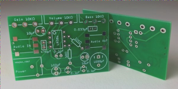
1. The milling cutter used in PCB manufacturing is also known as the gong knife.
2. It is employed in the post-processing stage of the PCB (or during frame pressing).
3. Its primary purpose is to cut the manufactured circuit board into individual PCBs or SPNLs, which are then shipped to the customer.
4. This ensures that the product meets the customer’s ultimate size requirements.
5. The tool is specifically designed for cutting, with the blade and force direction oriented transversely, similar to a drill bit, but with the drill bit’s force and cutting direction applied at the tip.

