As one of the most critical components in the modern electronics industry, PCB boards are used in nearly all electronic products and are often referred to as “the mother of electronic system products.” With the growing demand for higher PCB quality, information traceability systems such as marking characters, barcodes, and QR codes have emerged to better manage and control product quality during production.
Currently, PCB marking is primarily achieved through two methods: silk screen printing and laser marking.
Traditional silk-screen printing involves using a precisely made graphic screen and applying external pressure to force ink through the mesh of the screen, which then prints onto the surface of the circuit board. The unprinted areas of the screen block the ink from passing through, leaving blank spaces on the board. The printed ink forms characters, logos, patterns, and other markings. While this method is cost-effective and quick, it has several drawbacks: the marking quality is often coarse, the markings can easily wear off, it is unsuitable for small PCBs, and the chemicals used may have some level of toxicity.

Laser marking utilizes high-energy-density lasers to locally irradiate the PCB surface, causing the material to either vaporize or discolor, thereby leaving a permanent mark. This non-contact process can create highly detailed two-dimensional codes, even on small formats, ensuring exceptional precision and quality. Additionally, the markings are resistant to wear from extreme temperatures, chemical exposure, and external friction. No chemical substances are required, and the process has no negative impact on personnel safety or the environment.
Using a dedicated PCB laser marking machine, with its precision and flexibility, can overcome the limitations of screen printing, significantly boosting production efficiency and yield, while lowering costs and reducing environmental impact. As a result, laser marking is rapidly becoming the preferred method for PCB labeling and is widely applied in industries such as digital products, wearable devices, and automotive circuit boards.
Have you mastered the methods and techniques for PCB recognition?
Since PCB layouts can appear relatively “chaotic,” the following methods and strategies can help improve the speed of image recognition:
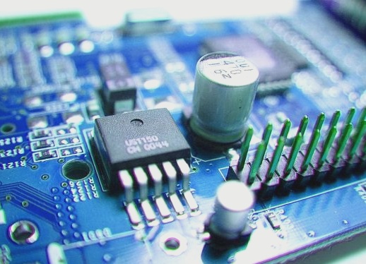
1. Certain components have distinctive physical characteristics that make them easy to identify, such as integrated circuits, power amplifier tubes, switches, and transformers.
2. For integrated circuits, identification can be made based on the type printed on the IC, enabling easy location of specific components.
While there are no strict rules for the distribution and arrangement of components, those within the same functional unit tend to be grouped together.
3. Some unit circuits exhibit recognizable features that make them easier to identify. For instance, rectifier circuits often contain more diodes, while power amplifier tubes are typically accompanied by heat sinks. The largest capacitors and components with the highest capacity are often filter capacitors.
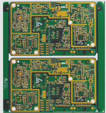
4. When locating the ground wire, the large-area copper foil on the PCB is usually the ground plane, which is typically interconnected across the entire board. Additionally, the metal casing of certain components may also be grounded. In some designs, ground connections are made between circuit boards, but it is important to note that when connectors between boards are not engaged, the ground connection may be blocked. This should be carefully considered during troubleshooting.
5. When comparing the PCB diagram to the actual circuit board, ensure that both the diagram and the board are aligned with the same orientation. This will save time by eliminating the need to adjust the direction for each comparison, streamlining the recognition process.
6. To better observe the connections between components and the copper traces on the PCB, use a lamp to shine light from the side of the copper foil. This makes it easier to see the connections from the component side, eliminating the need to flip the board constantly. Continuously flipping the PCB not only creates inconvenience but can also damage the leads or other delicate connections on the board.
Currently, PCB marking is primarily achieved through two methods: silk screen printing and laser marking.
Traditional silk-screen printing involves using a precisely made graphic screen and applying external pressure to force ink through the mesh of the screen, which then prints onto the surface of the circuit board. The unprinted areas of the screen block the ink from passing through, leaving blank spaces on the board. The printed ink forms characters, logos, patterns, and other markings. While this method is cost-effective and quick, it has several drawbacks: the marking quality is often coarse, the markings can easily wear off, it is unsuitable for small PCBs, and the chemicals used may have some level of toxicity.
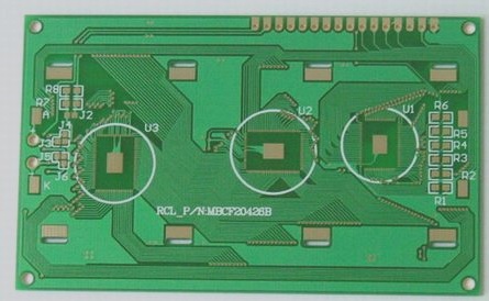
Laser marking utilizes high-energy-density lasers to locally irradiate the PCB surface, causing the material to either vaporize or discolor, thereby leaving a permanent mark. This non-contact process can create highly detailed two-dimensional codes, even on small formats, ensuring exceptional precision and quality. Additionally, the markings are resistant to wear from extreme temperatures, chemical exposure, and external friction. No chemical substances are required, and the process has no negative impact on personnel safety or the environment.
Using a dedicated PCB laser marking machine, with its precision and flexibility, can overcome the limitations of screen printing, significantly boosting production efficiency and yield, while lowering costs and reducing environmental impact. As a result, laser marking is rapidly becoming the preferred method for PCB labeling and is widely applied in industries such as digital products, wearable devices, and automotive circuit boards.
Have you mastered the methods and techniques for PCB recognition?
Since PCB layouts can appear relatively “chaotic,” the following methods and strategies can help improve the speed of image recognition:
1. Certain components have distinctive physical characteristics that make them easy to identify, such as integrated circuits, power amplifier tubes, switches, and transformers.
2. For integrated circuits, identification can be made based on the type printed on the IC, enabling easy location of specific components.
While there are no strict rules for the distribution and arrangement of components, those within the same functional unit tend to be grouped together.
3. Some unit circuits exhibit recognizable features that make them easier to identify. For instance, rectifier circuits often contain more diodes, while power amplifier tubes are typically accompanied by heat sinks. The largest capacitors and components with the highest capacity are often filter capacitors.
4. When locating the ground wire, the large-area copper foil on the PCB is usually the ground plane, which is typically interconnected across the entire board. Additionally, the metal casing of certain components may also be grounded. In some designs, ground connections are made between circuit boards, but it is important to note that when connectors between boards are not engaged, the ground connection may be blocked. This should be carefully considered during troubleshooting.
5. When comparing the PCB diagram to the actual circuit board, ensure that both the diagram and the board are aligned with the same orientation. This will save time by eliminating the need to adjust the direction for each comparison, streamlining the recognition process.
6. To better observe the connections between components and the copper traces on the PCB, use a lamp to shine light from the side of the copper foil. This makes it easier to see the connections from the component side, eliminating the need to flip the board constantly. Continuously flipping the PCB not only creates inconvenience but can also damage the leads or other delicate connections on the board.

