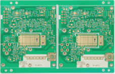
1. Years of valuable experience tell us that when dealing with via stubs, the most effective approach is to route the device on the surface layer to the lower layer, and route the device from the bottom layer to the upper layer, thereby minimizing the stub length. However, is there ever a situation where no matter which layer you route to, the stub length still cannot be sufficiently minimized?
2. Indeed, such a situation does exist, and it occurs quite frequently. In an ideal device layout, we prefer to place high-speed signal transceiver chips on the same side, either on the surface or the bottom. The rationale is simple: when we route from the pin on the surface layer to the inner layer, as long as we go to the lower layer (if the device is placed on the surface layer, or the opposite if placed on the bottom layer), the resulting vias will have relatively short stubs, improving signal transmission quality. And let’s not always bring up back drilling. This approach ensures signal quality while saving cost and simplifying the process. I believe no one would oppose that, right?
3. However, there are cases where high-speed signals cannot have both devices on the same side, leading to scenarios where these high-speed traces are overlooked. Do you think that, as long as we prioritize transmission, the best solution is to place them on the surface? Some issues can’t even be guaranteed by concubines, let alone PCB engineers! For instance, consider a device with high-speed traces on both sides of a pin…
4. Such devices do exist, and they are quite common. One such device, which is the focus of today’s discussion, is the PCIe gold finger. It is encountered in many PCIe daughter card designs and features a double-sided pad structure. Recently, we’ve been working extensively with PCIe signals, particularly in the rapidly growing field of artificial intelligence.
5. The highlighted TX link (How do you distinguish between TX or RX? Check the capacitor) is on the bottom layer, while our main chip is placed on the surface layer. This results in internal routing that seems to have no clear preference for which layer to route. Regardless of whether it’s placed on the upper or lower layer, one of the vias will still have a long stub. At this point, I can imagine how conflicted the PCB engineer feels, much like the situation depicted in the image below…
6. Now that we’ve set the stage, let’s dive into the case study that this article addresses. This signal follows the PCIe 3.0 protocol (8Gbps), and the board thickness is 2.0mm. In the first version of the design, the customer asked if we could avoid back drilling to save costs. Our high-speed engineer didn’t immediately suggest back drilling, but noted that the via stub was approximately 60mil, which is still acceptable for 8Gbps signals. The customer, though skeptical, approved the board design, and fortunately, after testing, it passed the PCIe performance test (with the daughter card inserted into the base) with no transmission issues.
7. Once everything was confirmed to be fine, the customer initiated the second version of the design. Although there were changes to other routing areas, the PCIe portion of the schematic remained unchanged. The initial assumption was that simply copying the PCIe layout from the first version would be sufficient. However, since the lower traces had to be adjusted to accommodate higher-speed signals, it was no longer possible to route them on the bottom layer as in the previous version. The PCB designer figured that the long via stub would be inevitable regardless of the routing, so they chose to route the trace on the upper layer, symmetrical to the previous bottom layer routing. The second version of the link looked like this (the difference between the two versions will be examined later, and comparing them will help clarify the impact of different routing layers).
8. As mentioned earlier, regardless of whether the routing is on the top or bottom layer, a long via stub is unavoidable. At first glance, the two versions may appear similar, as they still have both long and short via stubs. But is this really the case?
Let’s compare the two cases through simulation, and the transmission loss yields a rather surprising conclusion: it’s actually the same. As shown below: After thorough verification by the high-speed engineers, it was confirmed that there really are two curves, and they are exactly identical. The red curve is completely overlapped by the green one…
Upon further reflection, this makes sense. For a linear time-invariant system, the results should indeed be the same. The theory doesn’t require much elaboration, but if you’re curious, you can explore it further. Simply put, from the perspective of the final reception, the first instance is identical, and the order of the long and short stubs does not matter when the stub length is the same. The energy transmitted to the receiving end through oscillation remains the same. So it seems that in such cases, it doesn’t matter whether you move from the bottom layer to the top or vice versa.
Often, when you arrive at a conclusion that seems correct, it needs to withstand scrutiny from others. For instance, a colleague suggested adding a transceiver model to check if the eye diagram remains the same. That’s a good suggestion because, for many people, S-parameters are much less intuitive than time-domain waveforms or eye diagrams. After adding the transceiver model for simulation, we quickly overturned the initial conclusion…
PCB manufacturers were surprised to find that the gap was much larger than expected, with the eye height differing by more than 50 mV. Both cases appeared to have good waveforms, but in the PCIE link, this only applies to the daughter card portion. Once the base board is plugged in, the receiving margin becomes very small, highlighting a significant gap.
After the surprise wore off, we revisited the return loss of both links and eventually identified the difference.
From the perspective of return loss, the results of version one were indeed better than version two, which explains the discrepancy in the eye diagrams. Therefore, in situations where via stubs are present, the choice of routing layer has a significant impact, and we can no longer rely on the traditional approach of using the lower or upper layer. Instead, specific issues need to be analyzed in detail.
If you have any PCB manufacturing needs, please do not hesitate to contact me.Contact me