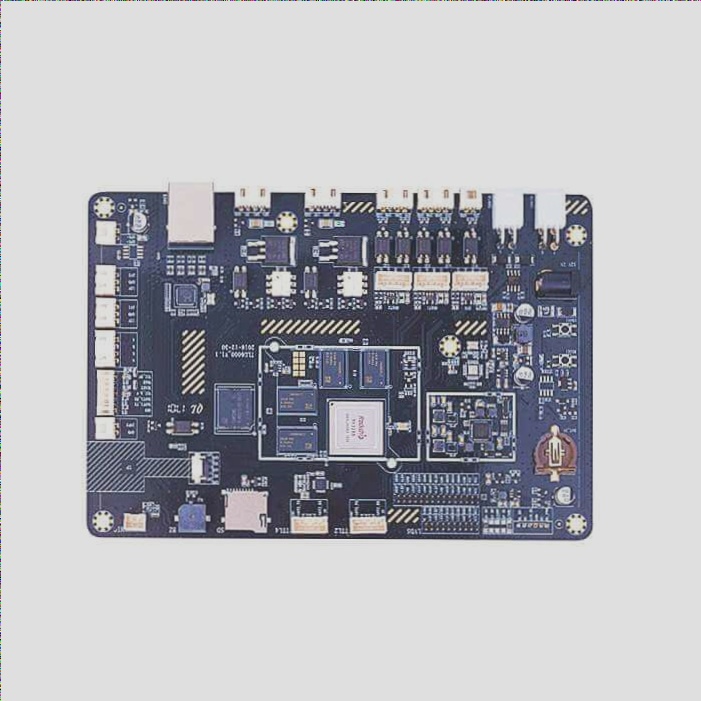
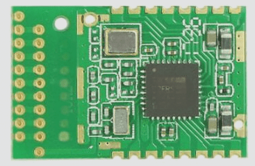
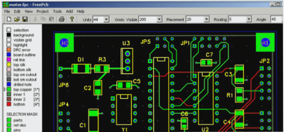
PCBs are composed of fiberglass, copper foil, and other metal parts bonded together by epoxy resin and insulated with a resistant layer. The color visible on the surface of the circuit board is derived from the solder film.
Perhaps you’ve noticed substances adhering to the circuit board’s surface; however, don’t mistake them for mere decoration. A sophisticated circuit board lacking high-quality components accurately affixed to its surface won’t function as intended. Printed circuit boards equipped with components are termed assembled circuit boards (assembled PCBs), and the manufacturing process is known as printed circuit board assembly or PCBA. In contrast, PCBs devoid of electronic components on their surfaces are referred to as bare boards. Copper wires on bare boards, known as traces, establish electrical connections between connectors and electronic elements, ultimately enabling the circuit board to function according to its design.

1. So, how are these assembled printed circuit boards made? PCB assembly (PCBA) is both simple and complex. It’s simple because it involves just a few automatic and manual steps, yet it’s complex because each step is crucial; even a minor deviation can lead to disastrous results. As modern electronics push towards miniaturization, every aspect of the assembly process demands meticulous attention to detail. To provide insight into the PCB assembly process, we’ll delve into each step in this article.
2. There are two primary modern PCB assembly technologies: Surface Mount Technology (SMT) and Through-Hole Technology (THT). SMT is chiefly used for assembling sensitive components like small resistors or diodes by placing them directly onto the circuit board’s surface. These components, known as surface mount devices (SMDs), are mounted through an automated process. SMT can accommodate small-sized components and integrated circuits (ICs). For instance, at WellCircuits, we can mount components as small as 01005, which is smaller than a pencil tip.
3. On the other hand, through-hole technology suits components with wires or pins, which are inserted into holes on the circuit board. Additional leads are then soldered to the opposite side of the board. Through-hole assembly is ideal for larger components such as capacitors.
4. Due to the distinctions between surface mount and through-hole techniques, they each follow unique assembly processes. This article will outline the PCBA assembly process, combining insights from both technologies.
5. Before formally commencing PCBA, preparatory work is essential. This involves evaluating the circuit board design’s functionality, primarily through Design for Manufacturability (DFM) inspection.
6. Circuit board assembly companies typically require comprehensive circuit board design documentation and specific assembly instructions. This documentation enables them to identify potential issues that could impact the circuit board’s function or manufacturability, a critical aspect of DFM inspection.
7. DFM inspection scrutinizes all design specifications for circuit boards. Its aim is to identify missing, redundant, or potentially problematic features that could compromise the final product’s functionality. For instance, inadequate spacing between components could lead to short circuits or even render the product unusable.
8. By preemptively identifying potential issues, DFM checks minimize manufacturing costs and prevent unexpected expenses by reducing the number of defective circuit boards. WellCircuits offers complimentary manufacturability design inspection, ensuring cost savings for our customers while upholding product quality and yield.
9. The first step in SMT assembly is uniformly applying solder paste to the circuit board’s pads, specifically targeting component areas. Precision in paste application is achieved through a stainless steel mesh with precise perforations aligned with the circuit board design.
10. Solder paste, a gray metallic substance comprising tiny metal balls, is a mixture of solder and flux. The flux facilitates solder melting and bonding to the surface. In a professional PCB assembly line, the solder paste is accurately applied to the designated areas using a mechanical fixture and an applicator.
11. After applying solder paste, the circuit board proceeds to the pickup machine, which automatically places surface-mount devices (SMDs) onto the printed solder paste circuit board. This process, once manual, has evolved into an automated procedure, significantly enhancing efficiency and accuracy.
12. The pickup and placing machine utilizes vacuum clamps to handle the circuit board and position components precisely. Components are then placed onto the solder paste in predetermined locations, ensuring accuracy and consistency.
13. Following component placement, the solder paste and surface-mount components are secured to the circuit board through a process called reflow. This involves melting the solder paste at high temperatures, cooling it, and permanently bonding the surface-mount elements to the board.
14. After reflow soldering, the assembled circuit board undergoes thorough inspection to ensure quality and functionality. Various inspection methods are employed, including manual inspection, automatic optical detection (AOI), and X-ray detection, each suited to different production scales and complexities.
15. Final inspection and functional testing are crucial post-assembly steps to verify the circuit board’s performance. Functional testing simulates real-world operation to assess whether the board meets specified requirements. Any deviations from expected performance indicate a failed test, warranting further investigation and rectification.
16. Printed circuit board assembly using Through-Hole Technology (THT) combines manual and automatic procedures. Professional engineers manually place electronic components according to the PCB design document, ensuring adherence to installation standards and quality requirements.
17. Once components are placed, the circuit board undergoes automatic inspection to verify correct component placement before soldering. Any discrepancies can be promptly corrected to prevent defects.
18. In the THT assembly process, wave soldering is employed to solder through-hole components onto the circuit board. The board moves through a wave of liquid solder, ensuring secure attachment of wire connections.
19. Subsequent to soldering, the THT assembly undergoes inspection and testing to confirm performance and quality. This comprehensive approach ensures that assembled circuit boards meet stringent standards for reliability and functionality.
20. Despite the meticulous assembly process, the finished circuit board may appear pristine but can harbor contaminants. Cleaning the circuit board after soldering is crucial to remove flux residue and any other impurities that could compromise performance or aesthetics.
21. WellCircuits prioritizes cleanliness by employing stainless steel high-pressure cleaning equipment with deionized water. This ensures thorough removal of residues without posing any threat to the circuit board. After cleaning, compressed air is used for rapid drying, preparing the PCBs for packaging and transportation.


