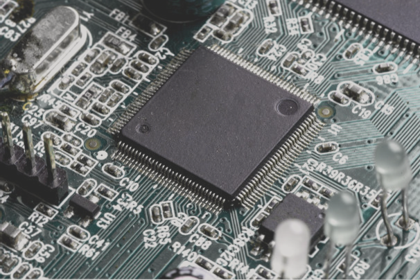
Common Issues in PCBA Processing
-
Short Circuits
Short circuits in PCBA manufacturing happen when two solder joints connect unintentionally, creating an unintended electrical path. Factors like solder joint proximity, incorrect soldering direction, or poor PCB design can contribute to this issue. Proper component placement and optimized soldering processes can help prevent short circuits.
-
Cold Solder Joints (Empty Soldering)
Cold solder joints occur when there is no proper solder connection between a component and the PCB. Reasons include unclean solder pads or poor alignment. To avoid cold joints, ensure clean pads, proper alignment, and correct flux and solder paste usage.
-
Solder Bridges (False Soldering)
Solder bridges happen when solder appears to connect a component lead and a pad but fails to form a proper electrical connection. Causes include rosin contamination or inadequate heating during soldering. Proper flux, solder paste, and heat application are crucial for reliable connections.
These issues can be mitigated through careful handling, effective soldering techniques, and attention to detail during the PCBA manufacturing process. Quality training, process control, and material usage are vital for producing high-quality PCBA products.
Common PCB Soldering Defects and Solutions
-
Cold Welding (Undissolved Tin)
Cold welding occurs due to low soldering temperature or short soldering time, resulting in insufficient solder flow. Increasing temperature or flow time can enhance joint integrity.
-
Parts Detachment
Components may shift or detach post-soldering due to improper adhesive selection or curing. Check adhesive specifications and optimize soldering speed for better component adhesion.
-
Missing Components
Human error or process failures can lead to missing components during assembly. Implement a robust inspection system to ensure all components are correctly installed before soldering.
-
Component Damage
Components can sustain damage like breakage or material defects during soldering. Proper preheating and controlled cooling processes are essential to prevent damage.
-
Denudation
Denudation is a common issue in PCB assembly where components are not adequately covered or protected. This can lead to exposure and potential damage. Implementing proper encapsulation or conformal coating can help prevent denudation.
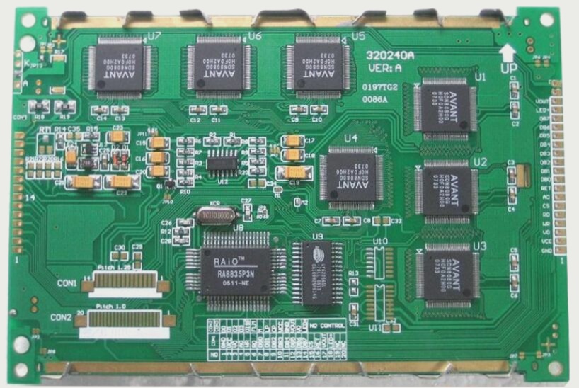
Common Issues in PCB Assembly and Solutions
- Denudation of Passive Components
- Tin Tip (Sharp Protrusions)
- Soldering Insufficiency
- Solder Balls (Beads)
- Open Circuit
- Tombstone Effect
- Wicking Effect
- Chip Components Turning White
- Reverse Polarity/Direction
- Component Shifting
- Excessive or Insufficient Glue
- Side Standing Components
Denudation affects components with poor plating, leading to terminal damage during soldering. Use components with better plating or adjust soldering parameters.
Sharp protrusions on solder joints can result from fast soldering or inadequate flux. Ensure proper soldering speed and uniform flux application.
Weak connections due to insufficient solder can be avoided by applying an adequate amount of solder paste.
Small accumulations of tin on PCBs can be caused by poor solder paste quality. Improve storage conditions and cleanliness to prevent solder balls.
Ensure electrical continuity by inspecting solder joints for missed connections or insufficient soldering.
Prevent chip components from lifting during soldering by ensuring uniform paste application and balanced thermal distribution.
Control solder rise along PLCC component leads by managing heating rates and preheating for uniform solder melting.
Optimize soldering processes to prevent solder flux from obscuring part markings during SMT assembly.
Ensure correct component orientation to avoid circuit malfunctions.
Prevent component movement during soldering by aligning parts carefully and controlling solder paste flow.
Proper adhesive application is crucial to prevent bonding issues and ensure component adhesion.
Align components correctly to avoid side standing issues caused by incorrect orientation or insufficient solder.
General Operational Guidelines for PCBA Boards and Components
- Maintain a Clean Work Environment
- Minimize Handling
- Avoid Direct Contact with Component Surfaces
Keep the work area clean and free from food, beverages, and smoking to prevent contamination.
Reduce assembly steps and replace gloves frequently to avoid contamination risks.
Best Practices for Handling PCB Components
- Avoid touching component surfaces with bare hands as oils and dirt can reduce solderability. Always handle components using tools or gloves to prevent contamination.
- Avoid Skin Care Products: Do not use oils, lotions, or silicone-containing detergents, as they can interfere with solderability and conformal coating adhesion. Use specialized cleaning agents designed for PCB assembly.
- Prevent Physical Damage: Do not stack PCBA boards, as this may cause physical damage. Use appropriate supports or racks to hold boards during assembly and testing.
- Handle ESD-Sensitive Components with Care: Ensure that PCBA boards and components sensitive to Electrostatic Discharge (ESD) are marked appropriately. Use ESD-protective workstations, equipment, and procedures to prevent damage during assembly and testing.
By following these guidelines and maintaining a consistent production process, you can prevent contamination and physical damage, ensuring the long-term reliability and performance of PCBA boards.
If you have any inquiries regarding PCB or PCBA, please don’t hesitate to contact me at info@wellcircuits.com.