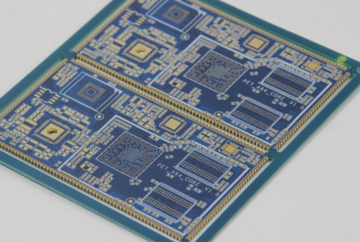
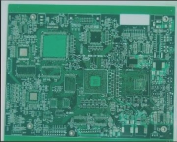
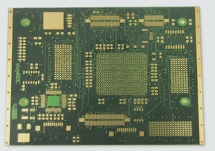
PCBA Processing Techniques and Methods
PCBA, or Printed Circuit Board Assembly, is a crucial step in the manufacturing process where a PCB is populated with components using SMT and DIP techniques.
Surface-Mounted Components in PCBA
- PCBA processing involves SMT surface assembly and DIP packaging, each with specific requirements based on component specifications.
- Surface assembly methods include full surface assembly, single-sided mixed assembly, and double-sided mixed assembly.
Full Surface Assembly Process
Full surface assembly populates both sides of the PCB with surface-mounted components (SMC/SMD). It can be single-sided or double-sided assembly.
Single-Sided Mixed Packaging
This process combines surface mount components (SMC/SMD) and through-hole components (THC) on one side of the PCB.
Double-Sided Mixed Installation
Here, SMC/SMD components are placed on both sides of the PCB, with THC on the main side or both sides.
Factors to Consider in PCBA Processing
- Assembly density and SMT line capabilities influence the selection of reflow soldering over wave soldering.
- Advantages of reflow soldering include precise control, lower thermal shock, self-positioning effect, and reduced defects.
- Reflow soldering offers better reliability, monitoring of solder composition, and ease of repair workloads.
In mixed assembly scenarios, where SMC/SMD and THC are on the same side, reflow soldering on side A and wave soldering on side B is recommended. For THC on side A and SMC/SMD on side B, a glue application and wave soldering process are used for side B.
High-Density Hybrid Assembly Techniques
When dealing with high-density hybrid assembly situations and minimal or no Through-Hole Components (THC), it is common to utilize double-sided solder paste printing and reflow soldering methods. In cases where a small amount of THC is required, it can be added as necessary.
If a significant number of THC components are located on side A of the assembly, the typical processing sequence involves the following steps:
- Printing solder paste on side A
- Reflow soldering
- Applying glue on side B
- Securing components
- Wave soldering
For any additional adjustments or inquiries, please don’t hesitate to reach out!