PCBA (Printed Circuit Board Assembly) is the process of assembling printed circuit boards with components and other parts to form a complete circuit board system. The following is a detailed analysis of the entire PCBA processing process, including design, procurement, manufacturing, assembly, and testing.
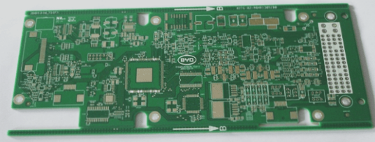
PCBA design is the initial step in the entire PCBA processing, involving both schematic and PCB design. Schematic design acts as the foundation of circuit design, utilizing software to create circuit diagrams and determine the connection and placement of each component. PCB design then transforms the schematic diagram into a PCB layout, organizing components on the circuit board and establishing circuit connections while determining the size, shape, and number of layers of the PCB.
During PCBA processing, a variety of components, circuit boards, and other auxiliary materials must be procured. When making purchases, factors such as component quality, price, delivery time, and supplier reliability must be considered. Furthermore, it is crucial to ensure that the purchased components meet design requirements and offer reliable and stable performance.
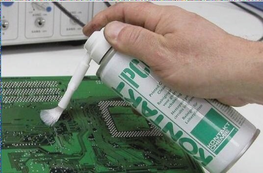
PCBA manufacturing involves transforming PCBs into printed circuit boards. Initially, the PCB is cut and punched to meet design specifications. Surface treatments such as gold plating and solder resist are chemically applied to protect the board surface and pads. Copper lamination procedures enhance board conductivity. Finally, screen printing is used to apply solder paste to the circuit board in preparation for component soldering.
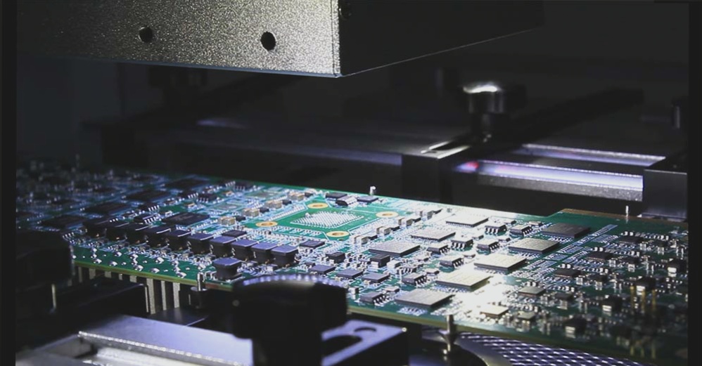
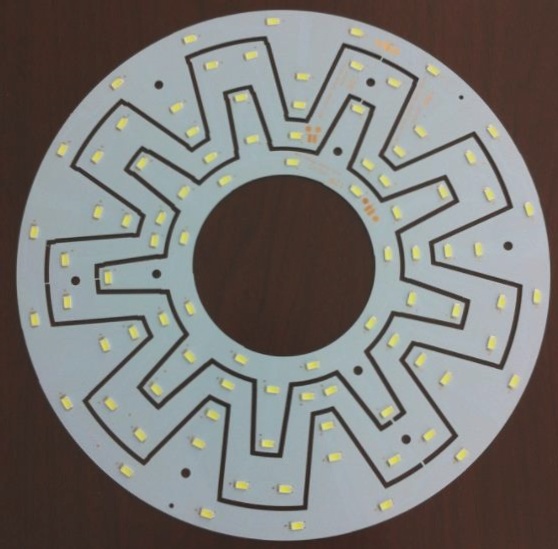
Assembly is the process of integrating components and circuit boards to form a complete circuit system. This process includes SMT (surface mount technology) and THT (through-hole technology), with SMT currently being the primary assembly method. Components are first accurately placed on the circuit board using automated equipment, followed by soldering to connect components to the board. Attention must be paid to proper component installation, soldering quality, and other factors to ensure the assembled circuit board’s reliability and stability.
Testing assesses the function and reliability of the PCBA. This process encompasses appearance inspection, functional testing, performance testing, and environmental testing. Appearance inspection checks for any physical damage to the PCBA. Functional testing evaluates circuit functionality through electrical tests. Performance testing assesses the PCBA’s performance under various conditions to confirm it meets requirements. Environmental testing exposes the PCBA to different conditions to verify its reliability and stability in diverse environments.
In conclusion, the PCBA processing journey includes various steps such as design, procurement, manufacturing, assembly, and testing. Each phase requires strict control to guarantee PCBA quality and reliability. Continuous process improvement and optimization are essential to enhance manufacturing efficiency and reduce costs. Only through meticulous control and optimization at each stage can high-quality PCBA products be produced.