Implementing Strain Gauge Measurements in PCB Production
1. In the past, PCB factories started requiring the use of Strain gages to measure the effects of stress on PCBA bending. This has now become a crucial inspection standard in PCB production.
2. Many R&D teams now consider Strain gauge as a key design reference, shifting focus from verifying process stress.
3. The next goal is to incorporate Strain gauge measurements in DQ tumble tests and drop tests.
4. The objective is to evaluate bending strain on the internal circuit board caused by impacts during tests, essential for validating design parameters.
5. Without this validation, even with efforts to minimize strain during assembly, products may fail upon reaching customers.
6. Failures could result in poor market reception for the products.
7. The aim is to advance Strain gauge measurement in R&D, driven by Shenzhen Grand Power’s interests.
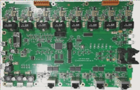
8. When facing BGA solder ball cracking issues, the immediate response is to enhance solder strength to prevent cracks.
Enhancing PCB Rigidity to Combat Impact Stress
1. Despite efforts to strengthen solder, it cannot fully withstand stress from board bending during falls. This raises doubts about electronic parts falling or solder cracking being a myth in the SMT process.
2. A shielding can was developed and designed to be directly welded to the circuit board, aiming to boost rigidity against bending issues from impact stress. Care was taken to ensure the welding does not extend to the soldering pad’s edge to form an effective solder arc.
3. Maintaining the shielding cover on the circuit board poses challenges, especially with equipment limitations in checking shielding alignment.
4. PCB engineers are tasked with measuring shielding cover offsets under a microscope and examining fillet shapes inside and outside the shielding case.
5. Engineers are requested to assess multiple shielding covers’ offsets using a microscope and inspect fillet shapes inside and outside the shielding cover.